LTC3452EUF#TRPBF Linear Technology, LTC3452EUF#TRPBF Datasheet
LTC3452EUF#TRPBF
Specifications of LTC3452EUF#TRPBF
Available stocks


Related parts for LTC3452EUF#TRPBF


LTC3452EUF#TRPBF Summary of contents
Page 1
... Cell Phones ■ Digital Cameras ■ PDAs ■ Portable Devices , LTC and LT are registered trademarks of Linear Technology Corporation. All other trademarks are the property of their respective owners. U TYPICAL APPLICATIO 5 × 20mA White LED Display + 200mA Camera Light Driver L 4.7µH V ...
Page 2
LTC3452 ABSOLUTE AXI U RATI GS (Note SW1, SW2, V Voltage ........... – 0. OUT LED to LED Voltage ... – 0. LED , ...
Page 3
ELECTRICAL CHARACTERISTICS The ● denotes specifications which apply over the full operating temperature range, otherwise specifications are 3.6V unless otherwise specified. (Note OUT PARAMETER LED Output Current Ratio (I /I ...
Page 4
LTC3452 W U TYPICAL PERFOR A CE CHARACTERISTICS Shutdown Current vs Temperature –55 ...
Page 5
W U TYPICAL PERFOR A CE CHARACTERISTICS PMOS R vs Temperature DS(ON) 325 300 V = 2.7V IN 275 V = 3.6V IN 250 225 V = 5.5V IN 200 V = 4.2V IN 175 150 125 –55 –35 –15 ...
Page 6
LTC3452 CTIO S (Pin 1): Signal Voltage Input Supply Pin (2.7V ≤ 5.5V). Recommended bypass capacitor to GND is 2.2µF ceramic or larger. Connect (Pin 2): Enable Input ...
Page 7
W BLOCK DIAGRA V IN 2. UNDERVOLTAGE UV LOCKOUT OVERTEMPERATURE OT PROTECTION BANDGAP 1.23V REFERENCE 1600mA BIAS V FB LOW POWER LED CURRENT SETTING AMP + 800mV I SETL – 3 ...
Page 8
LTC3452 U OPERATIO Buck-Boost DC-DC Converter The LTC3452 employs an LTC proprietary buck-boost DC/DC converter to generate the output voltage required to drive the LEDs. This architecture permits high-effi- ciency, low noise operation at input voltages above, below or equal ...
Page 9
U OPERATIO duty cycle DC . The input voltage V 4SW switch region begins is given by OUT 150 – • and the input voltage V where the four switch region ...
Page 10
LTC3452 U OPERATIO LED Current Setting Amps The maximum forward current per LED for all LEDs in a given bank is programmed by a single external resistor to ground at the corresponding I SETL,H following formulas: ⎛ ⎞ ...
Page 11
U U APPLICATIO S I FOR ATIO COMPONENT SELECTION Inductor Selection The high frequency operation of the LTC3452 allows the use of small surface mount inductors. The inductor cur- rent ripple is typically set to 20% to 40% of the ...
Page 12
LTC3452 U U APPLICATIO S I FOR ATIO Optional Schottky Diodes Schottky diodes across the synchronous switches B and D are not required, but provide a lower drop during the break-before-make time (typically 20ns) of the NMOS to PMOS transition, ...
Page 13
U U APPLICATIO S I FOR ATIO Although the LTC3452 can safely provide this current continuously, the external LED(s) may not be rated for this high a level of continuous current. Higher current levels in a single LED are generally ...
Page 14
LTC3452 U U APPLICATIO S I FOR ATIO Unused Outputs If fewer than 7 LED pins are to be used, unused LEDx pins should be connected The LTC3452 senses which OUT current source outputs are not being ...
Page 15
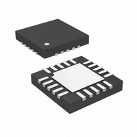
... SHADED AREA IS ONLY A REFERENCE FOR PIN 1 LOCATION ON THE TOP AND BOTTOM OF PACKAGE Information furnished by Linear Technology Corporation is believed to be accurate and reliable. However, no responsibility is assumed for its use. Linear Technology Corporation makes no represen- tation that the interconnection of its circuits as described herein will not infringe on existing patent rights Package 20-Lead Plastic QFN (4mm × ...
Page 16
... I = <1µA, OUT(MAX 4.5V 600µ 6µA, OUT(MAX 5.15V 825µ 0µA, OUT(MAX 34V 1.9mA <1µA, OUT(MAX 40V 5mA <16µA, OUT(MAX 40V 6.5mA <1µA, OUT(MAX 0406 • PRINTED IN THE USA © LINEAR TECHNOLOGY CORPORATION 2006 3452f ...