FAN3100TMPX Fairchild Semiconductor, FAN3100TMPX Datasheet
FAN3100TMPX
Specifications of FAN3100TMPX
Available stocks


Related parts for FAN3100TMPX


FAN3100TMPX Summary of contents
Page 1
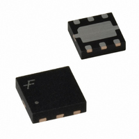
... DC-to-DC Converters Motor Control Functional Pin Configurations Figure 1. 2x2mm 6-Lead MLP (Top View) © 2007 Fairchild Semiconductor Corporation FAN3100 • Rev. 1.0.3 Description The FAN3100 2A gate driver is designed to drive 12V channel enhancement-mode MOSFET in low-side switching applications by providing high peak current pulses during the short switching intervals ...
Page 2
... Ordering Information Input Part Number Threshold FAN3100CMPX CMOS FAN3100CSX CMOS FAN3100TMPX TTL FAN3100TSX TTL Package Outlines Figure 3. 2x2mm 6-Lead MLP (Top View) Thermal Characteristics Package 6-Lead 2x2mm Molded Leadless Package (MLP) SOT23-5 Notes: 1. Estimates derived from thermal simulation; actual values depend on the application. ...
Page 3
... Power Ground (MLP only). For output drive circuit; separates switching noise from 5 PGND inputs. Output Logic IN+ IN− OUT ( ( Note: 7. Default input signal if no external connection is made. © 2007 Fairchild Semiconductor Corporation FAN3100 • Rev. 1.0.3 Pin Description 3 is above UVLO DD www.fairchildsemi.com ...
Page 4
... Block Diagrams Figure 5. Simplified Block Diagram (SOT23 Pin-out) © 2007 Fairchild Semiconductor Corporation FAN3100 • Rev. 1.0.3 Figure 6. Simplified Block Diagram (MLP Pin-out) 4 www.fairchildsemi.com ...
Page 5
... Absolute Maximum Ratings. Symbol V Supply Voltage Range DD V Input Voltage IN+, IN Operating Ambient Temperature A © 2007 Fairchild Semiconductor Corporation FAN3100 • Rev. 1.0.3 Parameter Human Body Model, JEDEC JESD22-A114 Charged Device Model, JEDEC JESD22-C101 Parameter 5 Min. Max. Unit -0.3 20 ...
Page 6
... RVS Note: 8. Lower supply current due to inactive TTL circuitry. 9. Not tested in production. 10. See Timing Diagrams of Figure 7 and Figure 8. © 2007 Fairchild Semiconductor Corporation FAN3100 • Rev. 1.0.3 = -40°C to +125°C. Currents are defined as positive into the device and J Conditions (8) FAN3100C FAN3100T ...
Page 7
... Timing Diagrams Output Input © 2007 Fairchild Semiconductor Corporation FAN3100 • Rev. 1.0.3 90% 10% V INH V INL RISE Figure 7. Non-Inverting 7 t FALL www.fairchildsemi.com ...
Page 8
... Typical characteristics are provided at 25°C and V Figure 9. I (Static) vs. Supply Voltage DD Figure 11. I (No-Load) vs. Frequency DD Figure 13. I (1nF Load) vs. Frequency DD © 2007 Fairchild Semiconductor Corporation FAN3100 • Rev. 1.0.3 =12V unless otherwise noted. DD Figure 10. I (Static) vs. Supply Voltage DD Figure 12. I (No-Load) vs. Frequency DD Figure 14 ...
Page 9
... Typical Performance Characteristics Typical characteristics are provided at 25°C and V Figure 15. I (Static) vs. Temperature DD Figure 17. Input Thresholds vs. Supply Voltage Figure 19. Input Thresholds % vs. Supply Voltage © 2007 Fairchild Semiconductor Corporation FAN3100 • Rev. 1.0.3 =12V unless otherwise noted. DD Figure 16. I (Static) vs. Temperature DD Figure 18 ...
Page 10
... Typical Performance Characteristics Typical characteristics are provided at 25°C and V Figure 20. CMOS Input Thresholds vs. Temperature Figure 22. UVLO Thresholds vs. Temperature Figure 24. Propagation Delay vs. Supply Voltage © 2007 Fairchild Semiconductor Corporation FAN3100 • Rev. 1.0.3 =12V unless otherwise noted. DD Figure 21. TTL Input Thresholds vs. Temperature Figure 23 ...
Page 11
... Typical Performance Characteristics Typical characteristics are provided at 25°C and V Figure 26. Propagation Delay vs. Supply Voltage Figure 28. Propagation Delay vs. Temperature Figure 30. Propagation Delay vs. Temperature © 2007 Fairchild Semiconductor Corporation FAN3100 • Rev. 1.0.3 =12V unless otherwise noted. DD Figure 27. Propagation Delay vs. Supply Voltage Figure 29 ...
Page 12
... Typical characteristics are provided at 25°C and V Figure 32. Fall Time vs. Supply Voltage Figure 34. Rise and Fall Time vs. Temperature Figure 35. Rise / Fall Waveforms with 1nF Load © 2007 Fairchild Semiconductor Corporation FAN3100 • Rev. 1.0.3 =12V unless otherwise noted. DD Figure 33. Rise Time vs. Supply Voltage Figure 36 ...
Page 13
... Figure 39. Quasi-Static Source Current with 4.7µF ceramic IN 1µF 1kHz ceramic Figure 41. Quasi-Static I OUT © 2007 Fairchild Semiconductor Corporation FAN3100 • Rev. 1.0.3 =12V unless otherwise noted. DD =12V Figure 38. Quasi-Static Sink Current with V DD =8V Figure 40. Quasi-Static Sink Current with V DD 470µF Al ...
Page 14
... MOSFET turn-on or turn-off interval, the driver supplies high peak current for fast switching even though the Miller plateau is not present. This situation © 2007 Fairchild Semiconductor Corporation FAN3100 • Rev. 1.0.3 often occurs in synchronous rectifier applications because the body diode is generally conducting before the MOSFET is switched on ...
Page 15
... The localized C contain the high peak current pulses within this driver- MOSFET circuit, preventing them from disturbing the sensitive analog circuitry in the PWM controller. © 2007 Fairchild Semiconductor Corporation FAN3100 • Rev. 1.0.3 Figure 43. Current Path for MOSFET Turn-On acts to ...
Page 16
... Non-Inverting Configuration In the inverting driver application shown in Figure 46, the IN+ pin is tied high. Pulling the IN+ pin to GND forces the output low, regardless of the state of the IN- pin. Figure 46. Dual-Input Driver Enabled, Inverting Configuration © 2007 Fairchild Semiconductor Corporation FAN3100 • Rev. 1.0.3 OUT ...
Page 17
... MOSFET on and off at the switching frequency. The power dissipation that results from driving a MOSFET at a specified gate- © 2007 Fairchild Semiconductor Corporation FAN3100 • Rev. 1.0.3 source voltage, V switching frequency, f ...
Page 18
... Typical Application Diagrams Figure 49. Forward Converter, Primary-Side Gate Drive (MLP Package Shown) Figure 50. Driver for Two-Transistor Forward Converter Gate Transformer Figure 52. Programmable Time Delay Using CMOS Input © 2007 Fairchild Semiconductor Corporation FAN3100 • Rev. 1.0.3 Figure 51. Secondary Synchronous Rectifier Driver 18 ...
Page 19
... Dual 4A +4.3A / -2.8A FAN3225C Dual 4A +4.3A / -2.8A FAN3225T Dual 4A +4.3A / -2.8A Note: 11. Typical currents with OUT at 6V and V © 2007 Fairchild Semiconductor Corporation FAN3100 • Rev. 1.0.3 Input (11) Threshold CMOS Single Channel of Two-Input/One-Output TTL Single Channel of Two-Input/One-Output CMOS Dual Inverting Channels + Dual Enable ...
Page 20
... Package drawings are provided as a service to customers considering Fairchild components. Drawings may change in any manner without notice. Please note the revision and/or date on the drawing and contact a Fairchild Semiconductor representative to verify or obtain the most recent revision. Package specifications do not expand the terms of Fairchild’s worldwide terms and conditions, specifically the warranty therein, which covers Fairchild products. Always visit Fairchild Semiconductor’ ...
Page 21
... Package drawings are provided as a service to customers considering Fairchild components. Drawings may change in any manner without notice. Please note the revision and/or date on the drawing and contact a Fairchild Semiconductor representative to verify or obtain the most recent revision. Package specifications do not expand the terms of Fairchild’s worldwide terms and conditions, specifically the warranty therein, which covers Fairchild products. Always visit Fairchild Semiconductor’ ...
Page 22
... Fairchild Semiconductor Corporation FAN3100 • Rev. 1.0.3 22 www.fairchildsemi.com ...