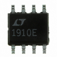
LT1910ES8#PBF Linear Technology, LT1910ES8#PBF Datasheet - Page 6

LT1910ES8#PBF
Manufacturer Part Number
LT1910ES8#PBF
Description
IC MOSFET DRIVER HIGH-SIDE 8SOIC
Manufacturer
Linear Technology
Datasheet
1.LT1910ES8PBF.pdf
(12 pages)
Specifications of LT1910ES8#PBF
Configuration
High-Side
Input Type
Non-Inverting
Delay Time
220µs
Number Of Configurations
1
Number Of Outputs
1
Voltage - Supply
8 V ~ 48 V
Operating Temperature
-40°C ~ 85°C
Mounting Type
Surface Mount
Package / Case
8-SOIC (3.9mm Width)
Lead Free Status / RoHS Status
Lead free / RoHS Compliant
Current - Peak
-
High Side Voltage - Max (bootstrap)
-
Available stocks
Company
Part Number
Manufacturer
Quantity
Price
PIN FUNCTIONS
LT1910
Information). A maximum of 10kΩ can be inserted between
a drain-sense resistor and the SENSE pin. If current sensing
is not required, the SENSE pin is tied to supply.
BLOCK DIAGRAM
OPERATION
The LT1910 GATE pin has two states, off and on. In the off
state it is held LOW, while in the on state it is pumped to
12V above the supply by a self-contained 750kHz charge
pump. The off state is activated when either the IN pin is
below 0.8V or the TIMER pin is below 2.9V. Conversely,
for the on state to be activated, the IN pin must be above
2V and the TIMER pin must be above 2.9V.
The IN pin has approximately 200mV of hysteresis. If it is
left open, the IN pin is held LOW by a 75k resistor. Under
normal conditions, the TIMER pin is held a diode drop
above 2.9V by a 14μA pull-up current source. Thus the
TIMER pin automatically reverts the GATE pin to the on
state if the IN pin is above 2V.
6
TIMER
IN
V
+
75k
14μA
3.3V
2.9V
1.4V
75k
(Refer to the Block Diagram)
–
+
+
–
+
–
FAULT
+
–
1.4V
V
rent for the LT1910, the V
connection for the current-sense comparator. The V
must be connected to the positive side of the drain-sense
resistor for proper current-sensing operation.
The SENSE pin normally connects to the drain of the power
MOSFET, which returns through a low value drain-sense
resistor to supply. In order for the sense comparator to
accurately sense the MOSFET drain current, the V
must be connected directly to the positive side of the
drain-sense resistor. When the GATE pin is on and the
MOSFET drain current exceeds the level required to gener-
ate a 65mV drop across the drain-sense resistor, the sense
comparator activates a pull-down NPN which rapidly pulls
the TIMER pin below 2.9V. This in turn causes the timer
comparator to override the IN pin and set the GATE pin
to the off state, thus protecting the power MOSFET. When
the TIMER pin is pulled below 3.3V, the fault comparator
+
(Pin 8): In addition to providing the operating cur-
+
–
V
+
–
+
SENSE
+
65mV
CHARGE PUMP
OSCILLATOR
pin also serves as the Kelvin
AND
250Ω
1910 BD
GATE
+
+
1910fa
pin
pin


