SI9910DY-T1-E3 Vishay, SI9910DY-T1-E3 Datasheet
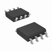
IC MOSFET DVR ADAPTIVE PWR 8SOIC

SI9910DY-T1-E3

Manufacturer Part Number
SI9910DY-T1-E3
Description
IC MOSFET DVR ADAPTIVE PWR 8SOIC
Manufacturer
Vishay
Type
High Sider
Datasheets

Specifications of SI9910DY-T1-E3

Configuration
High-Side
Input Type
Non-Inverting
Delay Time
120ns
Current - Peak
1A
Number Of Configurations
1
Number Of Outputs
1
High Side Voltage - Max (bootstrap)
500V
Voltage - Supply
10.8 V ~ 16.5 V
Operating Temperature
-40°C ~ 85°C
Mounting Type
Surface Mount
Package / Case
8-SOIC (3.9mm Width)
Rise Time
50 ns
Fall Time
35 ns
Supply Voltage (min)
10.8 V
Supply Current
0.5 mA
Maximum Power Dissipation
700 mW
Maximum Operating Temperature
+ 85 C
Mounting Style
SMD/SMT
Bridge Type
Half Bridge
Minimum Operating Temperature
- 40 C
Number Of Drivers
1
Device Type
MOSFET
Peak Output Current
1A
Input Delay
120ns
Output Delay
135ns
Supply Voltage Range
10.8V To 16.5V
Driver Case Style
SOIC
No. Of Pins
8
Operating Temperature Range
-40°C To +85°C
Lead Free Status / RoHS Status
Lead free / RoHS Compliant
Lead Free Status / RoHS Status
Lead free / RoHS Compliant, Lead free / RoHS Compliant
Other names
SI9910DY-T1-E3TR

Available stocks

Company
Part Number
Manufacturer
Quantity
Price
Part Number:
SI9910DY-T1-E3
Manufacturer:
TI
Quantity:
87
Part Number:
SI9910DY-T1-E3
Manufacturer:
VISHAY/威世
Quantity:
20 000
Company:
Part Number:
SI9910DY-T1-E3
Quantity:
11 589
DESCRIPTION
The Si9910 Power MOSFET driver provides optimized gate
drive signals, protection circuitry and logic level interface. Very
low quiescent current is provided by a CMOS buffer and a
high-current emitter-follower output stage. This efficiency
allows operation in high-voltage bridge applications with
“bootstrap” or “charge-pump”
techniques.
The non-inverting output configuration minimizes current
drain for an n-channel “on” state. The logic input is internally
diode clamped to allow simple pull-down in high-side drives.
Document Number: 70009
S-42043—Rev. H, 15-Nov-04
1. Patent Number 484116.
FEATURES
D dv/dt and di/dt Control
D Undervoltage Protection
D Short-Circuit Protection
FUNCTIONAL BLOCK DIAGRAM
INPUT
V
DD
V
DS
Delay
2-ms
D t
D Low Quiescent Current
D CMOS Compatible Inputs
Adaptive Power MOSFET Driver
Undervoltage/
Overcurrent
rr
Protection
floating power supply
Shoot-Through Current Limiting
V
SS
Fault protection circuitry senses an undervoltage or output
short-circuit condition and disables the power MOSFET.
Addition of one external resistor limits maximum di/dt of the
external Power MOSFET. A fast feedback circuit may be used
to limit shoot-through current during t
time) in a bridge configuration.
The Si9910 is available in both standard and lead (Pb)-free
8-pin plastic DIP and SOIC packages which are specified to
operate over the industrial temperature range of −40 _C to
85 _C.
D Compatible with Wide Range of MOSFET Devices
D Bootstrap and Charge Pump Compatible
(High-Side Drive)
PULL-DOWN
PULL-UP
DRAIN
I
SENSE
* Typical Values
1
*100 kW
*250 W
R3
R2
C1
Vishay Siliconix
rr
*2 to 5 pF
(diode reverse recovery
*0.1 W
R1
www.vishay.com
Si9910
1

Related parts for SI9910DY-T1-E3

SI9910DY-T1-E3 Summary of contents

Page 1

... The Si9910 is available in both standard and lead (Pb)-free 8-pin plastic DIP and SOIC packages which are specified to operate over the industrial temperature range of − _C. DRAIN PULL-UP PULL-DOWN I SENSE Typical Values Si9910 Vishay Siliconix (diode reverse recovery rr R3 *100 *250 W R1 *0.1 W www.vishay.com 1 ...

Page 2

... Si9910 Vishay Siliconix ABSOLUTE MAXIMUM RATINGS Voltages Referenced to V Pin SS V Supply Range . . . . . . . . . . . . . . . . . . . . . . . . . . . . . . . . . . . DD Pin Pin Input Current . . . . . . . . . . . . . . . . . . . . . . . . . . . . . . . . . . . . . . . . . . . . . Peak Current ( Storage Temperature . . . . . . . . . . . . . . . . . . . . . . . . . . . . . . . . . . Stresses beyond those listed under “Absolute Maximum Ratings” may cause permanent damage to the device. These are stress ratings only, and functional operation of the device at these or any other conditions beyond those indicated in the operational sections of the specifications is not implied ...

Page 3

... IN ( PLH 10% OUT PIN CONFIGURATIONS AND ORDERING INFORMATION PDIP INPUT DRAIN 4 Top View Part Number Si9910DY Si9910DY-T1 Si9910DY-T1—E3 Si9910DJ Si9910DJ—E3 Document Number: 70009 S-42043—Rev. H, 15-Nov-04 90 PULL-UP 8 Pull-DOWN INPUT DRAIN 5 SENSE ORDERING INFORMATION Temperature Range −40 to 85_C Vishay Siliconix ...

Page 4

... Si9910 Vishay Siliconix PIN DESCRIPTION Pin Pin sense input for the maximum source-drain DS voltage limit. Two microseconds after a high transition on input pin 2, an internal timer enables the V DS(max) catastrophic overcurrent condition, excessive on-resistance, or insufficient gate-drive voltage can be sensed by limiting the maximum voltage drop across the power MOSFET. An external resistor (R3) is required to protect pin 1 from overvoltage during the MOSFET “ ...

Page 5

... C2 = Bootstrap Cap C3 = Chargepump Cap FIGURE 1. High-Voltage Half-Bridge with Si9910 Drivers Vishay Siliconix maintains worldwide manufacturing capability. Products may be manufactured at one of several qualified locations. Reliability data for Silicon Technology and Package Reliability represent a composite of all qualified locations. http://www.vishay.com/ppg?70009. Document Number: 70009 S-42043— ...

Page 6

... Vishay disclaims any and all liability arising out of the use or application of any product described herein or of any information provided herein to the maximum extent permitted by law. The product specifications do not expand or otherwise modify Vishay’ ...

Related keywords