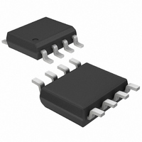
MAX5057BASA+ Maxim Integrated Products, MAX5057BASA+ Datasheet

MAX5057BASA+
Specifications of MAX5057BASA+
Related parts for MAX5057BASA+
MAX5057BASA+ Summary of contents
Page 1
... TDFN and SO Packages PART MAX5054AATA+ MAX5054AATA/V+ MAX5054BATA+ MAX5055AASA+ MAX5055BASA+ MAX5056AASA+ V OUT MAX5056BASA+ MAX5057AASA+ MAX5057BASA Exposed pad. /V Denotes an automotive qualified part. + Denotes a lead(Pb)-free/RoHS-compliant package. Selector Guide and Pin Configurations appear at end of data sheet. Features DD Ordering Information TEMP PIN- TOP RANGE ...
Page 2
Dual MOSFET Drivers ABSOLUTE MAXIMUM RATINGS (Voltages referenced to GND.) V ...............................................................................-0.3V to +18V DD INA+, INA-, INB+, INB- ...............................................-0.3V to +18V OUTA, OUTB...................................................-0. OUTA, OUTB Short-Circuit Duration ........................................10ms Continuous Source/Sink Current at OUT_ (P Continuous ...
Page 3
ELECTRICAL CHARACTERISTICS (continued 15V -40°C to +125°C, unless otherwise noted. Typical values are PARAMETER DRIVER OUTPUT (SOURCE) Driver Output Resistance Pulling Up Peak Output Current (Sourcing) Output-Voltage High LOGIC INPUT ...
Page 4
Dual MOSFET Drivers ELECTRICAL CHARACTERISTICS (continued 15V -40°C to +125°C, unless otherwise noted. Typical values are PARAMETER SYMBOL MATCHING CHARACTERISTICS Mismatch Propagation Delays from Inverting and Noninverting Inputs ...
Page 5
A I SUPPLY CURRENT DD-SW vs. TEMPERATURE 4 15V 250kHz 3.5 DUTY CYCLE = 50% BOTH CHANNELS SWITCHING 3.0 2.5 2.0 1.5 1.0 -50 -25 ...
Page 6
Dual MOSFET Drivers (T = +25°C, unless otherwise noted.) A DELAY MISMATCH BETWEEN 2 CHANNELS vs. TEMPERATURE 4.5V 10,000pF OUTPUT FALLING -50 -25 ...
Page 7
A LOGIC-INPUT VOLTAGE vs. OUTPUT VOLTAGE (V = 15V LOGIC-INPUT VOLTAGE vs. OUTPUT VOLTAGE (V = 15V vs. OUTPUT VOLTAGE DD _______________________________________________________________________________________ 4A, 20ns, Dual MOSFET Drivers Typical Operating ...
Page 8
Dual MOSFET Drivers MAX5054 PIN NAME 1 INA- Inverting Logic-Input Terminal for Driver A. Connect to GND when not used. 2 INB- Inverting Logic-Input Terminal for Driver B. Connect to GND when not used. 3 GND Ground 4 ...
Page 9
IN_ OUT_ t D-OFF1 IN_ D-OFF2 RISING MISMATCH = D-ON2 D-ON1 FALLING MISMATCH = D-OFF2 D-OFF1 Figure 1. Timing Diagram MAX5054 IN_- BREAK- BEFORE- MAKE ...
Page 10
Dual MOSFET Drivers Table 1. MAX5054 Truth Table INA+/INB+ INA-/INB- Low Low Low High High Low High High Table 2. MAX5055/MAX5056/MAX5057 Truth Table NONINVERTING IN_+ Low High INVERTING IN_- Low High The logic inputs are high impedance and ...
Page 11
Supply Bypassing and Grounding Pay extra attention to bypassing and grounding the MAX5054–MAX5057. Peak supply and output currents may exceed 8A when both drivers drive large external capacitive loads in phase. Supply voltage drops and ground shifts create forms of ...
Page 12
Dual MOSFET Drivers Both the SO-EP and TDFN-EP packages have an exposed pad on the bottom of their package. These pads are internally connected to GND. For the best thermal conductivity, solder the exposed pad to the V ...
Page 13
Figure 6. Schematic of a 48V Input, 3.3V at 15A Output Synchronously Rectified, Isolated Power Supply ______________________________________________________________________________________ 4A, 20ns, Dual MOSFET Drivers 13 ...
Page 14
Dual MOSFET Drivers TOP VIEW INA- 1 INB- 2 GND 3 OUTB 4 N.C. 1 INA+ 2 GND 3 INB+ 4 Selector Guide PIN- PART PACKAGE CMOS Dual Inverting DD MAX5054AATA 8 TDFN-EP* and Dual ...
Page 15
... Maxim cannot assume responsibility for use of any circuitry other than circuitry entirely embodied in a Maxim product. No circuit patent licenses are implied. Maxim reserves the right to change the circuitry and specifications without notice at any time. Maxim Integrated Products, 120 San Gabriel Drive, Sunnyvale, CA 94086 408-737-7600 ____________________ 15 © 2011 Maxim Integrated Products ...


