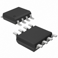
MAX5063AASA+ Maxim Integrated Products, MAX5063AASA+ Datasheet

MAX5063AASA+
Specifications of MAX5063AASA+
Related parts for MAX5063AASA+
MAX5063AASA+ Summary of contents
Page 1
... Noninverting MAX5062CASA Noninverting MAX5062DASA Noninverting Selector Guide continued at end of data sheet. ________________________________________________________________ Maxim Integrated Products For pricing, delivery, and ordering information, please contact Maxim/Dallas Direct! at 1-888-629-4642, or visit Maxim’s website at www.maxim-ic.com. 125V/2A, High-Speed, Half-Bridge MOSFET Drivers ♦ HIP2100/HIP2101 Pin Compatible (MAX5062A/ MAX5063A) ♦ ...
Page 2
High-Speed, Half-Bridge MOSFET Drivers ABSOLUTE MAXIMUM RATINGS (All voltages referenced to GND, unless otherwise noted IN_H, IN_L, IN_L+, IN_L-, IN_H+, IN_H-........-0.3V to +15V DD DL, BBM .....................................................-0. HS............................................................................-5V to +130V DH to HS.....................................................-0. ...
Page 3
ELECTRICAL CHARACTERISTICS (continued +8V to +12.6V GND = 0V, BBM = open BST +12V and T = +25°C.) (Note 1) DD BST A PARAMETER SYMBOL Logic-Input Current ...
Page 4
High-Speed, Half-Bridge MOSFET Drivers ELECTRICAL CHARACTERISTICS (continued +8V to +12.6V GND = 0V, BBM = open BST +12V and T = +25°C.) (Note 1) DD BST ...
Page 5
+12V and T DD BST UNDERVOLTAGE LOCKOUT (V AND V RISING) vs. TEMPERATURE DD BST 7.5 7.4 7.3 UVLO VDD 7.2 7.1 7.0 UVLO 6.9 BST 6.8 6.7 6.6 6.5 -40 -25 ...
Page 6
High-Speed, Half-Bridge MOSFET Drivers (Typical values are +12V and T DD BST V AND BST OPERATING SUPPLY DD CURRENT vs. FREQUENCY ...
Page 7
+12V and T DD BST FALL PROPAGATION DELAY vs. TEMPERATURE -40 -25 -10 5 ...
Page 8
High-Speed, Half-Bridge MOSFET Drivers PIN NAME 1 V Power Input. Bypass to GND with a parallel combination of 0.1µF and 1µF ceramic capacitor. DD Boost Flying Capacitor Connection. Connect a 0.1µF ceramic capacitor between BST and HS for the ...
Page 9
IN_L IN_L- IN_H IN_H MATCH1 D_ON2 D_ON1 MATCH2 D_ON3 D_ON1 Figure 1. Timing Characteristics for Noninverting and Inverting Logic Inputs ...
Page 10
High-Speed, Half-Bridge MOSFET Drivers Undervoltage Lockout Both the high- and low-side drivers feature undervolt- age lockout (UVLO). The low-side driver’s UVLO threshold is referenced to GND and pulls both driver outputs low when V falls below 6.8V. The high-side ...
Page 11
Topologies like the two-switch forward converter, where both high- and low-side switches are turned on and off simultaneously, can have the BBM function disabled by leaving BBM unconnected. When disabled, t cally 1ns. Driver Logic Inputs (IN_H, IN_L, IN_H+, IN_H-, ...
Page 12
High-Speed, Half-Bridge MOSFET Drivers EXTERNAL BBM DELAY PWM IN INH INL MAX5062B/MAX5062D/MAX5063B/MAX5063D/MAX5064 EXTERNAL BBM DELAY PWM IN INH INL MAX5062A/MAX5062C/MAX5063A/MAX5063C/MAX5064 Figure 3. Minimum Pulse-Width Behavior for High Duty-Cycle Input (Off-Time < t Applications ...
Page 13
C is the combined capacitive load at DH and L DL the supply voltage and f DD frequency of the converter. P includes the power dis- D sipated in the internal bootstrap diode. The internal power dissipation ...
Page 14
High-Speed, Half-Bridge MOSFET Drivers 12.6V DD PWM CONTROLLER PIN FOR PIN REPLACEMENT FOR THE HIP2100/HIP2101 Figure 4. MAX5062 Half-Bridge Conversion 12.6V DD PWM C BBM Figure 5. Synchronous Buck Converter 14 ...
Page 15
12.6V DD PWM Figure 6. Two-Switch Forward Conversion 12.6V DD PWM R C BBM BBM Figure 7. MAX5064 Half-Bridge Converter ______________________________________________________________________________________ 125V/2A, High-Speed, Half-Bridge MOSFET Drivers Typical Application Circuits (continued) C BST ...
Page 16
High-Speed, Half-Bridge MOSFET Drivers MAX5062A MAX5062C V /2 CMOS DD BST IN_H IN_L DL 6 GND SO/SO-EP MAX5063B/ MAX5063D TTL BST IN_H IN_L DL 6 GND SO/SO-EP TOP VIEW ...
Page 17
V = 125V IN R BBM PART HIGH-SIDE DRIVER MAX5063AASA Noninverting MAX5063BASA Noninverting MAX5063CASA Noninverting MAX5063DASA Noninverting Both Inverting and MAX5064AATC Noninverting Both Inverting and MAX5064BATC Noninverting Ordering Information (continued) TEMP PIN- PART RANGE PACKAGE -40°C to MAX5063AASA 8 SO ...
Page 18
High-Speed, Half-Bridge MOSFET Drivers (The package drawing(s) in this data sheet may not reflect the most current specifications. For the latest package outline information go to www.maxim-ic.com/packages.) 18 ______________________________________________________________________________________ Package Information PACKAGE OUTLINE 8L SOIC, .150" EXPOSED PAD 1 ...
Page 19
For the latest package outline information go to www.maxim-ic.com/packages.) ______________________________________________________________________________________ 125V/2A, High-Speed, Half-Bridge MOSFET Drivers Package Information (continued) 19 ...
Page 20
... Maxim cannot assume responsibility for use of any circuitry other than circuitry entirely embodied in a Maxim product. No circuit patent licenses are implied. Maxim reserves the right to change the circuitry and specifications without notice at any time. 20 ____________________Maxim Integrated Products, 120 San Gabriel Drive, Sunnyvale, CA 94086 408-737-7600 © 2007 Maxim Integrated Products Package Information (continued) ...


