LTC1165CS8#PBF Linear Technology, LTC1165CS8#PBF Datasheet
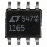
IC MOSFET DVR HI-SIDE TRPL 8SOIC

LTC1165CS8#PBF

Manufacturer Part Number
LTC1165CS8#PBF
Description
IC MOSFET DVR HI-SIDE TRPL 8SOIC
Manufacturer
Linear Technology
Datasheet

Specifications of LTC1165CS8#PBF

Configuration
High-Side
Input Type
Inverting
Delay Time
130µs
Number Of Configurations
3
Number Of Outputs
3
Voltage - Supply
1.8 V ~ 6 V
Operating Temperature
0°C ~ 70°C
Mounting Type
Surface Mount
Package / Case
8-SOIC (3.9mm Width)
Lead Free Status / RoHS Status
Lead free / RoHS Compliant
Current - Peak
-
High Side Voltage - Max (bootstrap)
-

Available stocks

Company
Part Number
Manufacturer
Quantity
Price
Company:
Part Number:
LTC1165CS8#PBFLTC1165CS8
Manufacturer:
LT
Quantity:
10 000
Company:
Part Number:
LTC1165CS8#PBFLTC1165CS8#TRPBF
Manufacturer:
LINEAR/凌特
Quantity:
20 000
FEATURE
A
TYPICAL
PPLICATI
PCMCIA Card 3.3V/5V Switch
2-Cell High-Side Load Switching
Boost Regulator Shutdown to Zero Standby Current
Replacing P-Channel Switches
Notebook Computer Power Management
Palmtop Computer Power Management
Portable Medical Equipment
Mixed 3.3V and 5V Supply Switching
Operates from 1.8V to 6V
0.01 A Standby Current
95 A Operating Current per Channel at 3.3V
Fully Enhances N-Channel Switches
No External Charge Pump Components
Built-In Gate Voltage Clamps
Easily Protected Against Supply Transients
Controlled Switching ON and OFF Times
Compatible with 5V, 3V and Sub-3V Logic Families
Available in 8-Pin SOIC
+
2-CELL
BATTERY
PACK
LTC1163 HAS NONINVERTING INPUTS
LTC1165 HAS INVERTING INPUTS
(1.8V TO 3V)
CONTROL
LOGIC
OR P
S
A
O
PPLICATI
+
U
IN1
IN2
IN3
2-Cell Triple High-Side Switch
10 F
S
LTC1163
LTC1165
GND
V
S
RFD14N05LSM
O
OUT1
OUT2
OUT3
U
2-CELL
LOAD
RFD14N05LSM
2-CELL
LOAD
RFD14N05LSM
LTC1163/65 • TA01
D
The LTC1163/LTC1165 triple low voltage MOSFET drivers
make it possible to switch supply or ground referenced
loads through inexpensive, low R
from as little as a 1.8V supply. The LTC1165 has inverting
inputs and makes it possible to directly replace P-channel
MOSFET switches while maintaining system drive polar-
ity. The LTC1163 has noninverting inputs.
Micropower operation, with 0.01 A standby current and
95 A operating current, coupled with a power supply
range of 1.8V to 6V, make the LTC1163/LTC1165 ideally
suited for 2- to 4-cell battery-powered applications. The
LTC1163/LTC1165 are also well suited for sub-3V, 3.3V
and 5V nominal supply applications.
The LTC1163/LTC1165 internal charge pumps boost the
gate voltage 8V above a 3.3V rail, fully enhancing inexpen-
sive N-channels for high- or low-side switch applications.
The LTC1163/LTC1165 are available in both an 8-pin DIP
and an 8-pin SOIC.
2-CELL
LOAD
Triple 1.8V to 6V High-Side
ESCRIPTIO
18
16
14
12
10
8
6
4
2
0
U
0
MOSFET Switch Gate Voltage
MOSFET Drivers
LTC1163/LTC1165
1
SUPPLY VOLTAGE (V)
2
DS(ON)
3
N-channel switches
4
LTC1163/65 • TA02
5
6
1

Related parts for LTC1165CS8#PBF

LTC1165CS8#PBF Summary of contents

Page 1

S FEATURE Operates from 1. 0.01 A Standby Current 95 A Operating Current per Channel at 3.3V Fully Enhances N-Channel Switches No External Charge Pump Components Built-In Gate Voltage Clamps Easily Protected Against Supply Transients Controlled Switching ON ...

Page 2

LTC1163/LTC1165 BSOLUTE Supply Voltage ......................................................... 7V Any Input Voltage .......................... 7V to (GND – 0.3V) Any Output Voltage ....................... 20V to (GND – 0.3V) Current (Any Pin)................................................. 50mA U PACKAGE/ORDER I FOR ATIO ...

Page 3

ELECTRICAL C HARA TERISTICS C SYMBOL PARAMETER t Turn-OFF Time OFF The denotes specifications which apply over the full operating temperature range. Note 1: Quiescent current OFF is for all channels in OFF condition TYPICAL PERFOR A Standby ...

Page 4

LTC1163/LTC1165 W U TYPICAL PERFOR A Standby Supply Current – TEMPERATURE (°C) LTC1163/65 • TPC07 CTIO S Input Pins The LTC1163 is ...

Page 5

U OPERATIO Gate Charge Pump Gate drive for the power MOSFET is produced by an internal charge pump circuit which generates a gate volt- age substantially higher than the power supply voltage. The charge pump capacitors are included on chip ...

Page 6

LTC1163/LTC1165 U U APPLICATIO S I FOR ATIO 3.3V V LT1129-3 3 100k S OUT1 1/3 LTC1163 ON/OFF IN1 GND Figure 1. Powering a Large Capacitive Load managed by the system regulator required ...

Page 7

... F Information furnished by Linear Technology Corporation is believed to be accurate and reliable. However, no responsibility is assumed for its use. Linear Technology Corporation makes no represen- tation that the interconnection of its circuits as described herein will not infringe on existing patent rights. U 2-Cell to 3.3V, 5V and 12V High-Side Switch/Converter with 0 ...

Page 8

... LT/GP 1093 10K REV 0 • PRINTED IN USA LINEAR TECHNOLOGY CORPORATION 1993 0.250 ± 0.010 (6.350 ± 0.254) 0.150 – 0.157 (3.810 – 3.988) ...

Related keywords