NJW4301D NJR, NJW4301D Datasheet
NJW4301D
Specifications of NJW4301D


Related parts for NJW4301D


NJW4301D Summary of contents
Page 1
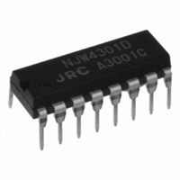
... Low Saturation Output (Vsat=±0.5V ● Supply Current (35mA MAX.) ● 2 channel BTL Output ● Mute Function ● Bi-MOS Technology ● Package Outline DIP16, SDMP30 ■ BLOCK DIAGRAM Ver.2003-12-09 ■ PACKAGE OUTLINE . at I =300mA) MAX O NJW4301D NJW4301M (Package DIP-16 ...
Page 2
ABSOLUTE MAXIMUM RATINGS (T PARAMETER Supply Voltage Operating Current Mute Terminal Current Power Dissipation Operating Temperature Range Storage Temperature Range (note board. ■ ELECTRICAL CHARACTERISTICS (V PARAMETER 【ALL 】 Operating Supply Voltage Range Mute OFF Current ...
Page 3
PIN CONFIGURATION Ver.2003-12- ...
Page 4
TERMINAL EXPLANATION PIN NO. PIN NAME DIP-16 SDMP- GND OUT4 - ...
Page 5
TERMINAL EXPLANATION PIN NO. PIN NAME DIP-16 SDMP- VBout 16 7 VBin MUTE Ver.2003-12-09 FUNCTION An buffer amplifier output. An buffer amplifier input. Supply Voltage. An mute input. Pulldown by 50kΩ ...
Page 6
TERMINAL EXPLANATION PIN NO. PIN NAME DIP-16 SDMP- OUT1 6 18 OUT2 7 21 Vin1(-) 8 22 Vin1(+) - 6 - FUNCTION Output terminal of AMP.1. OUT1 signal is opposite phase against OUT2. Output terminal of AMP.2. ...
Page 7
TERMINAL EXPLANATION PIN NO. PIN NAME DIP-16 SDMP- Vin2(+) 10 25 Vin2(-) 11 28 OUT3 Ver.2003-12-09 FUNCTION Inverting input terminal of AMP.3. Non-inverting input terminal of AMP.3. Output terminal of AMP.3. INSIDE EQUIVALENT CIRCUIT - 7 - ...
Page 8
APPLICATION CIRCUITS - 8 - NJW4301 (DIP-16) Application Circuit NJW4301 (SDMP-30) Application Circuit Ver.2003-12-09 ...
Page 9
TYPICAL CHARACTERISTICS Output Offset Voltage vs. Operating Voltage Operating Current vs. Operating Voltage Output Voltage vs. Output Current Ver.2003-12-09 Output Offset Voltage vs.Operating Voltage Output Voltage Range vs. Output Current - 9 - ...
Page 10
TYPICAL CHARACTERISTICS Total Harmonic Distortion vs. Output Power Total Harmonic Distortion vs. Frequency - 10 - Total Harmonic Distortion vs. Output Power Total Harmonic Distortion vs. Frequency [CAUTION] The specifications on this databook are only given for information , ...