IR2104STRPBF International Rectifier, IR2104STRPBF Datasheet
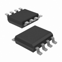
IC DRIVER HIGH/LOW SIDE 8SOIC

IR2104STRPBF

Manufacturer Part Number
IR2104STRPBF
Description
IC DRIVER HIGH/LOW SIDE 8SOIC
Manufacturer
International Rectifier
Datasheet

Specifications of IR2104STRPBF

Configuration
Half Bridge
Input Type
Non-Inverting
Delay Time
680ns
Current - Peak
210mA
Number Of Configurations
1
Number Of Outputs
2
High Side Voltage - Max (bootstrap)
600V
Voltage - Supply
10 V ~ 20 V
Operating Temperature
-40°C ~ 125°C
Mounting Type
Surface Mount
Package / Case
8-SOIC (3.9mm Width)
Number Of Drivers
2
Driver Configuration
Invert/Non-Invert
Driver Type
High and Low Side
Input Logic Level
CMOS/LSTTL
Rise Time
170ns
Fall Time
90ns
Propagation Delay Time
820ns
Operating Supply Voltage (max)
20V
Peak Output Current
360uA
Power Dissipation
625mW
Operating Supply Voltage (min)
10V
Turn Off Delay Time
60fs
Turn On Delay Time (max)
60ps
Operating Temp Range
-40C to 125C
Operating Temperature Classification
Automotive
Mounting
Surface Mount
Pin Count
8
Package Type
SOIC
Module Configuration
Half Bridge
Input Delay
680ns
Output Delay
150ns
Supply Voltage Range
10V To 20V
Driver Case Style
SOIC
No. Of Pins
8
Rohs Compliant
Yes
Lead Free Status / RoHS Status
Lead free / RoHS Compliant
Other names
IR2104SPBFTR

Available stocks

Company
Part Number
Manufacturer
Quantity
Price
Part Number:
IR2104STRPBF
Manufacturer:
TI
Quantity:
1 400
Part Number:
IR2104STRPBF
Manufacturer:
International Rectifier
Quantity:
28 235
Part Number:
IR2104STRPBF
Manufacturer:
ST
0
Part Number:
IR2104STRPBF
Manufacturer:
IR
Quantity:
20 000
Part Number:
IR2104STRPBF
0
Company:
Part Number:
IR2104STRPBF
Quantity:
508
Company:
Part Number:
IR2104STRPBF
Quantity:
10 000
Company:
Part Number:
IR2104STRPBF
Quantity:
8 000
Company:
Part Number:
IR2104STRPBF
Quantity:
20 000
Part Number:
IR2104STRPBFIR2104STRPBF
0
www.irf.com
Features
Typical Connection
Description
The IR2104(S) are high voltage, high speed power
MOSFET and IGBT drivers with dependent high and low
side referenced output channels. Proprietary HVIC and
latch immune CMOS technologies enable ruggedized
monolithic construction. The logic input is compatible with standard CMOS or LSTTL output, down to 3.3V logic.
The output drivers feature a high pulse current buffer stage designed for minimum driver cross-conduction. The
floating channel can be used to drive an N-channel power MOSFET or IGBT in the high side configuration which
operates from 10 to 600 volts.
(Refer to Lead Assignment for correct pin configuration) This/These diagram(s) show electrical
connections only. Please refer to our Application Notes and DesignTips for proper circuit board layout.
Floating channel designed for bootstrap operation
Fully operational to +600V
Tolerant to negative transient voltage
dV/dt immune
Gate drive supply range from 10 to 20V
Undervoltage lockout
3.3V, 5V and 15V input logic compatible
Cross-conduction prevention logic
Internally set deadtime
High side output in phase with input
Shut down input turns off both channels
Matched propagation delay for both channels
Also available LEAD-FREE
SD
V
IN
CC
V
IN
SD
COM
CC
HO
LO
V
V
B
S
Product Summary
Packages
Deadtime (typ.)
t
on/off
V
HALF-BRIDGE DRIVER
8 Lead SOIC
OFFSET
V
I
IR2104S
O
OUT
+/-
(typ.)
IR2104
Data Sheet No. PD60046-S
130 mA / 270 mA
up to 600V
680 & 150 ns
600V max.
10 - 20V
520 ns
( S ) & (PbF)
8 Lead PDIP
IR2104
LOAD
TO
1

Related parts for IR2104STRPBF

IR2104STRPBF Summary of contents

Page 1

Features Floating channel designed for bootstrap operation Fully operational to +600V Tolerant to negative transient voltage dV/dt immune Gate drive supply range from 10 to 20V Undervoltage lockout 3.3V, 5V and 15V input logic compatible Cross-conduction prevention logic Internally set ...

Page 2

S ) & (PbF) IR2104 Absolute Maximum Ratings Absolute maximum ratings indicate sustained limits beyond which damage to the device may occur. All voltage parameters are absolute voltages referenced to COM. The thermal resistance and power dissipation ratings are ...

Page 3

Dynamic Electrical Characteristics 15V 1000 pF and T BIAS Symbol Definition t on Turn-on propagation delay t off Turn-off propagation delay t sd Shutdown propagation delay t r Turn-on ...

Page 4

S ) & (PbF) IR2104 Functional Block Diagram IN DEAD TIME & SHOOT-THROUGH PREVENTION SD Lead Definitions Symbol Description IN Logic input for high and low side gate driver outputs (HO and LO), in phase with HO Logic input ...

Page 5

Figure 1. Input/Output Timing Diagram SD 50 90% LO Figure 3. Shutdown Waveform Definitions IN (LO) 50% 50% IN (HO 10% MT 90% Figure 5. Delay Matching Waveform Definitions www.irf.com IN ...

Page 6

S ) & (PbF) IR2104 -50 - Temperature (°C) Figure ...

Page 7

Temperature (°C) Figure 8A. Shutdown Time vs Temperature ...

Page 8

S ) & (PbF) IR2104 ...

Page 9

Temperature (°C) Figure 14A. High Level Output vs Temperature ...

Page 10

S ) & (PbF) IR2104 -50 - Temperature (°C) Figure 17A. V Supply Current BS vs Temperature ...

Page 11

Max -50 - Temperature (°C) Figure 20A. Logic "0" Input Current vs Temperature 11 M ax. 10 Typ -50 - Temperature ...

Page 12

S ) & (PbF) IR2104 -50 - Temperature (°C) Figure 23A. Output ...

Page 13

0.25 [.010 0.25 [.010 NOTES: 1. DIMENSIONING & TOLERANC ING PER ASME Y14.5M-1994. 2. CONTROLLING DIMENSION: ...

Page 14

S ) & (PbF) IR2104 LEADFREE PART MARKING INFORMATION Part number Date code Pin 1 Identifier ? MARKING CODE P Lead Free Released Non-Lead Free Released Basic Part (Non-Lead Free) 8-Lead PDIP IR2104 order IR2104 8-Lead SOIC IR2104S order ...

Related keywords