LTC1156CN#PBF Linear Technology, LTC1156CN#PBF Datasheet
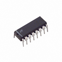
IC MOSFET DVR HI-SIDE QUAD 16DIP

LTC1156CN#PBF

Manufacturer Part Number
LTC1156CN#PBF
Description
IC MOSFET DVR HI-SIDE QUAD 16DIP
Manufacturer
Linear Technology
Datasheet

Specifications of LTC1156CN#PBF

Configuration
High-Side
Input Type
Non-Inverting
Delay Time
450µs
Number Of Configurations
4
Number Of Outputs
4
Voltage - Supply
4.5 V ~ 18 V
Operating Temperature
0°C ~ 70°C
Mounting Type
Through Hole
Package / Case
16-DIP (0.300", 7.62mm)
Number Of Drivers
4
Driver Type
High Side
Input Logic Level
CMOS/TTL
Operating Supply Voltage (max)
18V
Operating Supply Voltage (min)
4.5V
Operating Supply Voltage (typ)
15V
Turn Off Delay Time
60ps
Turn On Delay Time (max)
2ms
Operating Temp Range
0C to 70C
Operating Temperature Classification
Commercial
Mounting
Through Hole
Pin Count
16
Package Type
PDIP N
Lead Free Status / RoHS Status
Lead free / RoHS Compliant
Current - Peak
-
High Side Voltage - Max (bootstrap)
-
Lead Free Status / Rohs Status
Compliant
FEATURE
A
TYPICAL
ALL COMPONENTS SHOWN ARE SURFACE MOUNT. MINIMUM PARTS COUNT
SHOWN. CURRENT LIMITS CAN BE SET SEPARATELY AND TAILORED TO
INDIVIDUAL LOAD CHARACTERISTICS.
* IMS026 INTERNATIONAL MANUFACTURING SERVICES, INC. (401) 683-9700
PPLICATI
No External Charge Pump Components
Fully Enhances N-Channel Power MOSFETs
16 Microamps Standby Current
95 Microamps ON Current
Wide Power Supply Range 4.5V to 18V
Controlled Switching ON and OFF Times
Replaces P-Channel High Side Switches
Compatible with Standard Logic Families
Available in 16-pin SOL Package
Laptop Computer Power Switching
SCSI Termination Power Switching
Cellular Telephone Power Management
P-Channel Switch Replacement
Battery Charging and Management
Low Frequency H-Bridge Driver
Stepper Motor and DC Motor Control
CONTROL
OR P
LOGIC
5V
5V
+
S
A
10 F
O
PPLICATI
IN1
IN2
IN3
IN4
U
Laptop Computer Power Management
GND GND
LTC1156
S
V
S
V
S
DS1
DS2
DS3
DS4
G1
G2
G3
G4
O
U
0.1 F
Si9956DY
Si9956DY
100k
*30m
with Internal Charge Pump
Micropower MOSFET Driver
FLOPPY DISK
D
The LTC1156 quad High side gate driver allows using low
cost N-channel FETs for high side switching applications.
An internal charge pump boosts the gate drive voltage
above the positive rail, fully enhancing an N-channel MOS
switch with no external components. Micropower opera-
tion, with 16 A standby current and 95 A operating
current, allows use in virtually all systems with maximum
efficiency.
Included on chip is independent over-current sensing to
provide automatic shutdown in case of short circuits. A
time delay can be added to the current sense to prevent
false triggering on high in-rush current loads.
The LTC1156 operates off of a 4.5V to 18V supply and is
well suited for battery-powered applications, particularly
where micropower “sleep” operation is required.
The LTC1156 is available in both 16-pin DIP and 16-pin
SOL packages.
PERIPHERAL
HARD DISK
DISPLAY
DRIVE
DRIVE
ESCRIPTIO
1156 TA01
U
100
60
90
80
70
50
40
30
20
10
Quad High Side
0
0
V
T
IN1
J
= 25°C
= V
Standby Supply Current
IN2
5
SUPPLY VOLTAGE (V)
= V
IN3
= V
10
IN4
LTC1156
= 0V
15
LTC1156 G01
1
20

Related parts for LTC1156CN#PBF

LTC1156CN#PBF Summary of contents

Page 1

FEATURE S No External Charge Pump Components Fully Enhances N-Channel Power MOSFETs 16 Microamps Standby Current 95 Microamps ON Current Wide Power Supply Range 4.5V to 18V Controlled Switching ON and OFF Times Replaces P-Channel High Side Switches Compatible with ...

Page 2

LTC1156 BSOLUTE Supply Voltage ....................................................... 22V Input Voltage ..................... (V + 0.3V) to (GND – 0.3V) S Gate Voltage ....................... (V + 24V) to (GND – 0.3V) S Current (Any Pin)................................................. 50mA U ...

Page 3

ELECTRICAL C HARA TERISTICS C SYMBOL PARAMETER t Turn-OFF Time OFF t Short Circuit Turn-OFF Time SC The denotes specifications which apply over the full operating temperature range. Note 1: Both V pins (3 and 8) must be connected together, ...

Page 4

LTC1156 W U TYPICAL PERFOR A Turn-ON Time 1000 C = 1000pF GATE 900 800 700 600 500 400 300 200 100 SUPPLY VOLTAGE (V) 1156 ...

Page 5

U OPER ATIO A voltage regulator with low standby current provides continuous bias for the TTL to CMOS converters. The TTL to CMOS converter output enables the rest of the circuitry. In this way the power consumption is kept to ...

Page 6

LTC1156 O U TYPICAL A PPLICATI 24V to 30V Quad Industrial Switch with Thermal Shutdown 24V – 30V + 1N4746 18V 5V CONTROL LOGIC OR P Automotive Triple High Side Switch with Reverse Battery Interrupt, Short-Circuit and High-Voltage Transient Protection ...

Page 7

... For more Typical Applications, see LTC1155 data sheet. Information furnished by Linear Technology Corporation is believed to be accurate and reliable. However, no responsibility is assumed for its use. Linear Technology Corporation makes no represen- tation that the interconnection of circuits as described herein will not infringe on existing patent rights. ...

Page 8

... TYP 0.014 – 0.019 (0.356 – 0.483) TYP : 499-3977 0.770 (19.558 N16 1291 0.398 – 0.413 (10.109 – 10.490 0.394 – 0.419 SEE NOTE (10.008 – 10.643 LT/GP 0694 5K REV A • PRINTED IN USA LINEAR TECHNOLOGY CORPORATION 1994 SOL16 12/91 ...

Related keywords