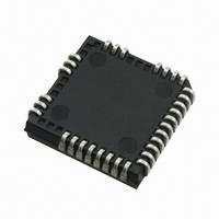
IRS2330DJPBF International Rectifier, IRS2330DJPBF Datasheet - Page 12

IRS2330DJPBF
Manufacturer Part Number
IRS2330DJPBF
Description
IC DVR 3-PHASE BRIDGE PLCC44
Manufacturer
International Rectifier
Datasheet
1.IRS2330JTRPBF.pdf
(36 pages)
Specifications of IRS2330DJPBF
Configuration
3 Phase Bridge
Input Type
Inverting
Delay Time
500ns
Current - Peak
250mA
Number Of Configurations
1
Number Of Outputs
3
High Side Voltage - Max (bootstrap)
600V
Voltage - Supply
10 V ~ 20 V
Operating Temperature
-40°C ~ 125°C
Mounting Type
Surface Mount
Package / Case
*
Lead Free Status / RoHS Status
Lead free / RoHS Compliant
Available stocks
Company
Part Number
Manufacturer
Quantity
Price
Company:
Part Number:
IRS2330DJPBF
Manufacturer:
International Rectifier
Quantity:
10 000
Matched Propagation Delays
The IRS233(0,2)(D) family of HVICs is designed with propagation delay matching circuitry.
response at the output to a signal at the input requires approximately the same time duration (i.e., t
side channels and the high-side channels. Additionally, the propagation delay for each low-side channel is matched when
compared to the other low-side channels and the propagation delays of the high-side channels are matched with each other.
The propagation turn-on delay (t
Input Logic Compatibility
The inputs of this IC are compatible with standard CMOS and TTL outputs. The IRS233(0,2)(D) family has been designed to
be compatible with 3.3 V and 5 V logic-level signals. The IRS233(0,2)(D) features an integrated 5.2 V Zener clamp on the
HIN, LIN, and ITRIP pins. Figure 6 illustrates an input signal to the IRS233(0,2)(D), its input threshold values, and the logic
state of the IC as a result of the input signal.
Undervoltage Lockout Protection
This family of ICs provides undervoltage lockout protection on both the V
V
waveform crosses the UVLO threshold (V
Upon power-up, should the V
voltage decreases below the V
condition and shutdown the high- and low-side gate drive outputs, and the FAULT pin will transition to the low state to inform
the controller of the fault condition.
Upon power-up, should the V
decreases below the V
shutdown the high-side gate drive outputs of the IC.
The UVLO protection ensures that the IC drives the external power devices only when the gate supply voltage is sufficient to
fully enhance the power devices. Without this feature, the gates of the external power switch could be driven with a low
voltage, resulting in the power switch conducting current while the channel impedance is high; this could result in very high
conduction losses within the power device and could lead to power device failure.
BS
(high-side circuitry) power supply. Figure 7 is used to illustrate this concept; V
www.irf.com
BSUV
threshold during operation, the undervoltage lockout circuitry will recognize a fault condition, and
BS
CC
voltage fail to reach the V
ON
CCUV-
voltage fail to reach the V
) of the IRS233(0,2)(D) is matched to the propagation turn-on delay (t
threshold during operation, the undervoltage lockout circuitry will recognize a fault
CCUV+/-
Figure 6: HIN & LIN input thresholds
or V
BSUV+/-
BSUV
) the undervoltage protection is enabled or disabled.
CCUV+
threshold, the IC will not turn-on. Additionally, if the V
threshold, the IC will not turn-on. Additionally, if the V
CC
(logic and low-side circuitry) power supply and the
CC
(or V
IRS233(0,2)(D)(S&J)PbF
BS
) is plotted over time and as the
With this feature, the IC’s
ON
, t
OFF
OFF
).
) for both the low-
BS
voltage
12
CC


