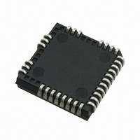
IRS2330DJPBF International Rectifier, IRS2330DJPBF Datasheet - Page 15

IRS2330DJPBF
Manufacturer Part Number
IRS2330DJPBF
Description
IC DVR 3-PHASE BRIDGE PLCC44
Manufacturer
International Rectifier
Datasheet
1.IRS2330JTRPBF.pdf
(36 pages)
Specifications of IRS2330DJPBF
Configuration
3 Phase Bridge
Input Type
Inverting
Delay Time
500ns
Current - Peak
250mA
Number Of Configurations
1
Number Of Outputs
3
High Side Voltage - Max (bootstrap)
600V
Voltage - Supply
10 V ~ 20 V
Operating Temperature
-40°C ~ 125°C
Mounting Type
Surface Mount
Package / Case
*
Lead Free Status / RoHS Status
Lead free / RoHS Compliant
Available stocks
Company
Part Number
Manufacturer
Quantity
Price
Company:
Part Number:
IRS2330DJPBF
Manufacturer:
International Rectifier
Quantity:
10 000
Truth Table: Undervoltage lockout and ITRIP
Table 2 provides the truth table for the IRS233(0,2)(D). The first line shows that the UVLO for V
FAULT output has gone low and the gate drive outputs have been disabled. V
greater than V
The second case shows that the UVLO for V
After V
case shows the normal operation of the HVIC. The fourth case illustrates that the ITRIP trip threshold has been reached and
that the gate drive outputs have been disabled and a fault has been reported through the fault pin. The fault output stays in the
low state until the fault condition has been removed by all LINx set to high state. Once the fault is removed, the voltage on the
FAULT pin will return to V
Advanced Input Filter
The advanced input filter allows an improvement in the input/output pulse symmetry of the HVIC and helps to reject noise
spikes and short pulses. This input filter has been applied to the HIN and LIN. The working principle of the new filter is shown
in Figures 12 and 13.
Figure 12 shows a typical input filter and the asymmetry of the input and output. The upper pair of waveforms (Example 1)
show an input signal with a duration much longer then t
input signal and t
t
Figure 13 shows the advanced input filter and the symmetry between the input and output. The upper pair of waveforms
(Example 1) show an input signal with a duration much longer then t
duration as the input signal.
then t
FIL,IN
Figure 10: Programming over-temperature protection
; the resulting output is approximately the difference between the input signal and t
www.irf.com
FIL,IN
BS
exceeds the V
; the resulting output is approximately the same duration as the input signal.
CCUV
Normal operation
FIL,IN
ITRIP fault
, the FAULT output returns to the high impedance state.
UVLO V
UVLO V
.
BSUV
The lower pair of waveforms (Example 2) show an input signal with a duration slightly longer then
CC
CC
BS
.
threshold , HO will stay low until the HVIC input receives a new falling transition of HIN. The third
The lower pair of waveforms (Example 2) show an input signal with a duration slightly longer
Table 2: IRS233(0,2)(D) UVLO, ITRIP & FAULT truth table
< V
VCC
15 V
15 V
15 V
CCUV
BS
has been tripped and that the high-side gate drive outputs have been disabled.
< V
VBS
15 V
15 V
---
BSUV
FIL,IN
; the resulting output is approximately the difference between the
Figure 11: Using over-current protection and over-temperature
>V
ITRIP
0 V
0 V
---
ITRIP
FIL,IN
High impedance
High impedance
; the resulting output is approximately the same
CCUV
FAULT
0
0
is not latched in this case and when V
FIL,IN
IRS233(0,2)(D)(S&J)PbF
protection
.
LIN
LIN
LO
0
0
CC
has been tripped; the
HIN
HO
0
0
0
15
CC
is


