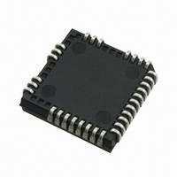
IRS2330DJPBF International Rectifier, IRS2330DJPBF Datasheet - Page 18

IRS2330DJPBF
Manufacturer Part Number
IRS2330DJPBF
Description
IC DVR 3-PHASE BRIDGE PLCC44
Manufacturer
International Rectifier
Datasheet
1.IRS2330JTRPBF.pdf
(36 pages)
Specifications of IRS2330DJPBF
Configuration
3 Phase Bridge
Input Type
Inverting
Delay Time
500ns
Current - Peak
250mA
Number Of Configurations
1
Number Of Outputs
3
High Side Voltage - Max (bootstrap)
600V
Voltage - Supply
10 V ~ 20 V
Operating Temperature
-40°C ~ 125°C
Mounting Type
Surface Mount
Package / Case
*
Lead Free Status / RoHS Status
Lead free / RoHS Compliant
Available stocks
Company
Part Number
Manufacturer
Quantity
Price
Company:
Part Number:
IRS2330DJPBF
Manufacturer:
International Rectifier
Quantity:
10 000
IRS233(0,2)(D)(S&J)PbF
Figure 17: Internal bootstrap MOSFET connection
Figure 18: Bootstrap MOSFET state diagram
A bootstrap MOSFET is suitable for most of the PWM modulation schemes and can be used either in parallel with the external
bootstrap network (i.e., diode and resistor) or as a replacement of it. The use of the integrated bootstrap as a replacement of
the external bootstrap network may have some limitations. An example of this limitation may arise when this functionality is
used in non-complementary PWM schemes (typically 6-step modulations) and at very high PWM duty cycle. In these cases,
superior performances can be achieved by using an external bootstrap diode in parallel with the internal bootstrap network.
Bootstrap Power Supply Design
For information related to the design of the bootstrap power supply while using the integrated bootstrap functionality of the
IRS233(0,2)D family, please refer to Application Note 1123 (AN-1123) entitled “Bootstrap Network Analysis: Focusing on the
Integrated Bootstrap Functionality.” This application note is available at www.irf.com.
For information related to the design of a standard bootstrap power supply (i.e., using an external discrete diode) please refer
to Design Tip 04-4 (DT04-4) entitled “Using Monolithic High Voltage Gate Drivers.” This design tip is available at www.irf.com.
Separate Logic and Power Grounds
The IRS233(0,2)(D) has separate logic and power ground pin (V
and VSO respectively) to eliminate some of the noise
SS
problems that can occur in power conversion applications. Current sensing shunts are commonly used in many applications
for power inverter protection (i.e., over-current protection), and in the case of motor drive applications, for motor current
measurements. In these situations, it is often beneficial to separate the logic and power grounds.
Figure 19 shows a HVIC with separate V
and VSO pins and how these two grounds are used in the system.
The V
is
SS
SS
used as the reference point for the logic and over-current circuitry; V
in the figure is the voltage between the ITRIP pin and
X
the V
pin. Alternatively, the VSO pin is the reference point for the low-side gate drive circuitry. The output voltage used to
SS
drive the low-side gate is V
-VSO; the gate-emitter voltage (V
) of the low-side switch is the output voltage of the driver
LO
GE
minus the drop across R
.
G,LO
www.irf.com
18


