ISL6594DCRZ Intersil, ISL6594DCRZ Datasheet - Page 9
ISL6594DCRZ
Manufacturer Part Number
ISL6594DCRZ
Description
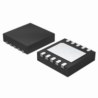
IC MOSFET DRVR SYNC BUCK 10-DFN
Manufacturer
Intersil
Datasheet
1.ISL6594DCBZ.pdf
(11 pages)
Specifications of ISL6594DCRZ
Configuration
High and Low Side, Synchronous
Input Type
PWM
Delay Time
10.0ns
Current - Peak
1.25A
Number Of Configurations
1
Number Of Outputs
2
High Side Voltage - Max (bootstrap)
36V
Voltage - Supply
6.8 V ~ 13.2 V
Operating Temperature
0°C ~ 85°C
Mounting Type
Surface Mount
Package / Case
10-DFN
Lead Free Status / RoHS Status
Lead free / RoHS Compliant
Available stocks
Company
Part Number
Manufacturer
Quantity
Price

Part Number:
ISL6594DCRZ
Manufacturer:
INTERSIL
Quantity:
20 000


vias. This combination of vias for vertical heat escape,
extended copper plane, and buried planes for heat
spreading allows the IC to achieve its full thermal potential.
Upper MOSFET Self Turn-On Effects at Start-up
Should the driver have insufficient bias voltage applied, its
outputs are floating. If the input bus is energized at a high
dV/dt rate while the driver outputs are floating, because of
self-coupling via the internal C
UGATE could momentarily rise up to a level greater than the
threshold voltage of the MOSFET. This could potentially turn
on the upper switch and result in damaging inrush energy.
Therefore, if such a situation (when input bus powered up
before the bias of the controller and driver is ready) could
conceivably be encountered, it is a common practice to
place a resistor (R
upper MOSFET to suppress the Miller coupling effect. The
value of the resistor depends mainly on the input voltage’s
rate of rise, the C
threshold of the upper MOSFET. A higher dV/dt, a lower
C
FET will require a smaller resistor to diminish the effect of
the internal capacitive coupling. For most applications, a
5kΩ to 10kΩ resistor is typically sufficient, not affecting
normal performance and efficiency.
The coupling effect can be roughly estimated using
Equation 5, which assume a fixed linear input ramp and
neglect the clamping effect of the body diode of the upper
drive and the bootstrap capacitor. Other parasitic
components such as lead inductances and PCB
capacitances are also not taken into account. These
equations are provided for guidance purpose only.
Therefore, the actual coupling effect should be examined
using a very high impedance (10MΩ or greater) probe to
ensure a safe design margin.
V
DS
R
GS_MILLER
=
/C
R
GS
UGPH
ratio, and a lower gate-source threshold upper
=
+
R
dV
------- R C
dt
GI
GD
UGPH
⋅
/C
⋅
GS
C
) across the gate and source of the
rss
rss
ratio, as well as the gate-source
⎛
⎜
⎜
⎜
⎜
⎝
1 e
=
–
9
GD
C
--------------------------------- -
dV
------ - R C
GD
dt
of the MOSFET, the
–
⋅
V
DS
⋅
iss
C
⎞
⎟
⎟
⎟
⎟
⎠
iss
=
C
GD
(EQ. 5)
+
C
GS
ISL6594D
FIGURE 5. GATE TO SOURCE RESISTOR TO REDUCE
PVCC
UPPER MOSFET MILLER COUPLING
DU
DL
PHASE
BOOT
UGATE
C
BOOT
G
R
C
GI
GD
C
GS
S
December 3, 2007
VIN
Q
UPPER
D
FN9282.1
C
DS
Related parts for ISL6594DCRZ
Image
Part Number
Description
Manufacturer
Datasheet
Request
R

Part Number:
Description:
Intersil Corporation [CMOS Serial Controller Interface]
Manufacturer:
Intersil Corporation
Datasheet:
Part Number:
Description:
Manufacturer:
Intersil Corporation
Datasheet:
Part Number:
Description:
357-036-542-201 CARDEDGE 36POS DL .156 BLK LOPRO
Manufacturer:
Intersil Corporation
Datasheet:
Part Number:
Description:
1024-Word x 4-Bit LSI Static RAM
Manufacturer:
Intersil Corporation
Datasheet:
Part Number:
Description:
General Purpose NPN Transistor Arrays FN341.4
Manufacturer:
Intersil Corporation
Datasheet:
Part Number:
Description:
CMOS 16-Bit Microprocessor
Manufacturer:
Intersil Corporation
Datasheet:
Part Number:
Description:
Manufacturer:
Intersil Corporation
Datasheet:
Part Number:
Description:
Manufacturer:
Intersil Corporation
Datasheet:
Part Number:
Description:
Manufacturer:
Intersil Corporation
Datasheet:
Part Number:
Description:
Manufacturer:
Intersil Corporation
Datasheet:
Part Number:
Description:
CMOS 6-Bit Latch and Decoder Memory Interfaces
Manufacturer:
Intersil Corporation
Datasheet:
Part Number:
Description:
CA3046General Purpose NPN Transistor Arrays
Manufacturer:
Intersil Corporation
Datasheet:
Part Number:
Description:
Manufacturer:
Intersil Corporation
Datasheet:
Part Number:
Description:
TR909 DLC/FLC SLIC with Low Power Standby
Manufacturer:
Intersil Corporation
Datasheet:
Part Number:
Description:
Manufacturer:
Intersil Corporation
Datasheet: