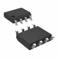
LM5109AMA/NOPB National Semiconductor, LM5109AMA/NOPB Datasheet

LM5109AMA/NOPB
Specifications of LM5109AMA/NOPB
*LM5109AMA/NOPB
LM5109AMA
Available stocks
Related parts for LM5109AMA/NOPB
LM5109AMA/NOPB Summary of contents
Page 1
... MOSFET n 1A peak output current (1.0A sink / 1.0A source) n Independent TTL compatible inputs Simplified Block Diagram © 2006 National Semiconductor Corporation n Bootstrap supply voltage to 108V DC n Fast propagation times (30 ns typical) n Drives 1000 pF load with 15ns rise and fall times n Excellent propagation delay matching (2 ns typical) ...
Page 2
Connection Diagrams Ordering Information Ordering Number Package Type LM5109AMA SOIC-8 LM5109AMAX SOIC-8 LM5109ASD LLP-8 LM5109ASDX LLP-8 Pin Descriptions Pin # Name SO-8 LLP Positive gate drive supply High side control input 3 3 ...
Page 3
... Absolute Maximum Ratings If Military/Aerospace specified devices are required, please contact the National Semiconductor Sales Office/ Distributors for availability and specifications (Note Junction Temperature Electrical Characteristics Specifications in standard typeface are for T perature range. Unless otherwise specified, V Symbol Parameter SUPPLY CURRENTS I V Quiescent Current ...
Page 4
Switching Characteristics Specifications in standard typeface are for T perature range. Unless otherwise specified, V Symbol Parameter LM5109A t Lower Turn-Off Propagation Delay (LI LPHL Falling to LO Falling) t Upper Turn-Off Propagation Delay (HI HPHL Falling to HO Falling) ...
Page 5
Typical Performance Characteristics V Operating Current vs Frequency DD Operating Current vs Temperature Quiescent Current vs Voltage HB Operating Current vs Frequency 20170204 Quiescent Current vs Temperature 20170206 Propagation Delay vs Temperature 20170208 5 20170205 20170207 20170209 www.national.com ...
Page 6
Typical Performance Characteristics LO and HO High Level Output Voltage vs Temperature Undervoltage Rising Thresholds vs Temperature Input Thresholds vs Temperature www.national.com (Continued) LO and HO Low Level Output Voltage vs Temperature 20170210 Undervoltage Hysteresis vs Temperature 20170214 Input Thresholds ...
Page 7
Timing Diagram Layout Considerations Optimum performance of high and low-side gate drivers cannot be achieved without taking due considerations during circuit board layout. The following points are emphasized: 1. Low ESR / ESL capacitors must be connected close to the ...
Page 8
Physical Dimensions Controlling dimension is inch. Values are millimeters. Notes: Unless otherwise specified. 1. Standard lead finish to be 200 microinches/5.08 micrometers minimum lead/tin (solder) on copper. 2. Dimension does not include mold flash. 3. Reference JEDEC ...
Page 9
... Physical Dimensions inches (millimeters) unless otherwise noted (Continued) Notes: Unless otherwise specified. 1. For solder thickness and composition, see “Solder Information” in the packaging section of the National Semiconductor web page (www.national.com). 2. Maximum allowable metal burr on lead tips at the package edges is 76 microns. ...


