ISL6597CRZ Intersil, ISL6597CRZ Datasheet - Page 4
ISL6597CRZ
Manufacturer Part Number
ISL6597CRZ
Description
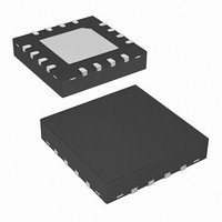
IC MOSFET DRVR DUAL SYNC 16-QFN
Manufacturer
Intersil
Datasheet
1.ISL6597CRZ.pdf
(10 pages)
Specifications of ISL6597CRZ
Configuration
High and Low Side, Synchronous
Input Type
Non-Inverting
Delay Time
18ns
Number Of Configurations
2
Number Of Outputs
4
High Side Voltage - Max (bootstrap)
36V
Voltage - Supply
4.5 V ~ 5.5 V
Operating Temperature
0°C ~ 70°C
Mounting Type
Surface Mount
Package / Case
16-VQFN Exposed Pad, 16-HVQFN, 16-SQFN, 16-DHVQFN
Lead Free Status / RoHS Status
Lead free / RoHS Compliant
Current - Peak
-


Absolute Maximum Ratings
Supply Voltage (PVCC, VCC) . . . . . . . . . . . . . . . . . . . . -0.3V to 7V
Input Voltage (V
BOOT Voltage (V
BOOT To PHASE Voltage (V
PHASE Voltage . . . . . . . . . . . . . . . . . . . . . GND - 0.3V to 15V (DC)
UGATE Voltage . . . . . . . . . . . . . . . . V
LGATE Voltage . . . . . . . . . . . . . . . GND - 0.3V (DC) to VCC + 0.3V
Ambient Temperature Range . . . . . . . . . . . . . . . . . .-40°C to +125°C
HBM ESD Rating . . . . . . . . . . . . . . . . . . . . . . . . . . . . . . . . . . . . .2kV
CAUTION: Stresses above those listed in “Absolute Maximum Ratings” may cause permanent damage to the device. This is a stress only rating and operation of the
device at these or any other conditions above those indicated in the operational sections of this specification is not implied.
+150°C max junction temperature is intended for short periods of time to prevent shortening the lifetime. Constantly operated at +150°C may shorten the life of the part.
NOTES:
Electrical Specifications
VCC SUPPLY CURRENT
Bias Supply Current
POR Rising
POR Falling
Hysteresis
BOOTSTRAP DIODE
Forward Voltage
VCTRL INPUT
Turn-On Threshold
Hysteresis
ENABLE INPUT
EN LOW Threshold
EN HIGH Threshold
EN Hysteresis
PWM INPUT
Sinking Impedance
Source Impedance
Tri-State Lower Threshold
Tri-State Upper Threshold
Tri-State Shutdown Holdoff Time
SWITCHING TIME (Note 3, See Figure 1)
UGATE Rise Time
LGATE Rise Time
UGATE Fall Time
1. θ
2. θ
JA
JC
, “case temperature” location is at the center of the package underside exposed pad. See Tech Brief TB379 for details.
is measured in free air with the component mounted on a high effective thermal conductivity test board with “direct attach” features.
GND -8V (<20ns Pulse Width, 10μJ) to 30V (<100ns)
GND - 2.5V (<20ns Pulse Width, 5μJ) to VCC + 0.3V
PARAMETER
EN
V
BOOT-GND
PHASE
, V
PWM
- 5V (<20ns Pulse Width, 10μJ) to V
) . . . . . . . . . . . . . . . -0.3V to VCC + 0.3V
). . . -0.3V to 25V (DC) or 36V (<200ns)
BOOT-PHASE
4
These specifications apply for T
PHASE
) . . . . . . -0.3V to 7V (DC)
- 0.3V (DC) to V
R
I
R
VCC+PVCC
-0.3V to 9V (<10ns)
SYMBOL
PWM_SNK
PWM_SRC
t
TSSHD
t
t
t
RU
V
RL
FU
F
PWM pin floating, V
F
V
V
V
V
V
V
V
BOOT
BOOT
Forward bias current = 2mA
PWM
VCC
VCC
VCC
VCC
VCC
VCC
VCC
ISL6597
A
= 3.3V (120mV Hysteresis)
= 5V (300mV Hysteresis)
= 3.3V (110mV Hysteresis)
= 5V (300mV Hysteresis)
= 5V, 3nF Load
= 5V, 3nF Load
= 5V, 3nF Load
= 300kHz, V
= 0°C to +70°C, unless otherwise noted
TEST CONDITIONS
Thermal Information
Thermal Resistance (Notes 1 and 2)
Maximum Junction Temperature . . . . . . . . . . . . . . . . . . . . . . +150°C
Maximum Storage Temperature Range . . . . . . . . . .-65°C to +150°C
Recommended Operating Conditions
Ambient Temperature Range. . . . . . . . . . . . . . . . . . . . 0°C to +70°C
Maximum Operating Junction Temperature. . . . . . . . . . . . . +125°C
Supply Voltage, VCC . . . . . . . . . . . . . . . . . . . . . . . . . . . . . 5V ±10%
VCC
VCC
QFN Package . . . . . . . . . . . . . . . . . .
= V
= V
PVCC
PVCC
= 5V
= 5V
1.00
1.40
1.65
3.00
MIN
100
2.6
0.3
2.5
-
-
-
-
-
-
-
-
-
-
-
-
-
TYP
1.34
1.60
1.15
1.55
1.85
3.18
350
400
100
260
1.7
3.4
3.0
0.6
2.8
3.5
3.5
8.0
8.0
8.0
80
θ
JA
(°C/W)
46
MAX
1.75
4.2
0.7
1.4
-
-
-
-
-
-
-
-
-
-
-
-
-
-
-
-
-
θ
JC
May 4, 2007
UNITS
FN9165.1
(°C/W)
8.5
mA
mV
mV
mV
μA
kΩ
kΩ
ns
ns
ns
ns
V
V
V
V
V
V
V
V
V
V
Related parts for ISL6597CRZ
Image
Part Number
Description
Manufacturer
Datasheet
Request
R

Part Number:
Description:
Dual Synchronous Rectified MOSFET Drivers
Manufacturer:
Intersil Corporation
Datasheet:
Part Number:
Description:
Intersil Corporation [CMOS Serial Controller Interface]
Manufacturer:
Intersil Corporation
Datasheet:
Part Number:
Description:
Manufacturer:
Intersil Corporation
Datasheet:
Part Number:
Description:
357-036-542-201 CARDEDGE 36POS DL .156 BLK LOPRO
Manufacturer:
Intersil Corporation
Datasheet:
Part Number:
Description:
1024-Word x 4-Bit LSI Static RAM
Manufacturer:
Intersil Corporation
Datasheet:
Part Number:
Description:
General Purpose NPN Transistor Arrays FN341.4
Manufacturer:
Intersil Corporation
Datasheet:
Part Number:
Description:
CMOS 16-Bit Microprocessor
Manufacturer:
Intersil Corporation
Datasheet:
Part Number:
Description:
Manufacturer:
Intersil Corporation
Datasheet:
Part Number:
Description:
Manufacturer:
Intersil Corporation
Datasheet:
Part Number:
Description:
Manufacturer:
Intersil Corporation
Datasheet:
Part Number:
Description:
Manufacturer:
Intersil Corporation
Datasheet:
Part Number:
Description:
CMOS 6-Bit Latch and Decoder Memory Interfaces
Manufacturer:
Intersil Corporation
Datasheet:
Part Number:
Description:
CA3046General Purpose NPN Transistor Arrays
Manufacturer:
Intersil Corporation
Datasheet:
Part Number:
Description:
Manufacturer:
Intersil Corporation
Datasheet:
Part Number:
Description:
TR909 DLC/FLC SLIC with Low Power Standby
Manufacturer:
Intersil Corporation
Datasheet: