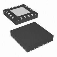
ISL6597CRZ Intersil, ISL6597CRZ Datasheet - Page 5

ISL6597CRZ
Manufacturer Part Number
ISL6597CRZ
Description
IC MOSFET DRVR DUAL SYNC 16-QFN
Manufacturer
Intersil
Datasheet
1.ISL6597CRZ.pdf
(10 pages)
Specifications of ISL6597CRZ
Configuration
High and Low Side, Synchronous
Input Type
Non-Inverting
Delay Time
18ns
Number Of Configurations
2
Number Of Outputs
4
High Side Voltage - Max (bootstrap)
36V
Voltage - Supply
4.5 V ~ 5.5 V
Operating Temperature
0°C ~ 70°C
Mounting Type
Surface Mount
Package / Case
16-VQFN Exposed Pad, 16-HVQFN, 16-SQFN, 16-DHVQFN
Lead Free Status / RoHS Status
Lead free / RoHS Compliant
Current - Peak
-
Electrical Specifications
NOTE:
Functional Pin Description
LGATE Fall Time
UGATE Turn-Off Propagation Delay
LGATE Turn-Off Propagation Delay
UGATE Turn-On Propagation Delay
LGATE Turn-On Propagation Delay
Tri-state to UG/LG Rising Propagation Delay
OUTPUT (Note 3)
Upper Drive Source Resistance
Upper Drive Sink Resistance
Lower Drive Source Resistance
Lower Drive Sink Resistance
3. Guaranteed by Characterization. Not 100% tested in production.
PACKAGE
PIN #
10
11
12
13
14
15
16
17
1
2
3
4
5
6
7
8
9
SYMBOL
PARAMETER
PHASE2
UGATE2
UGATE1
PHASE1
LGATE1
LGATE2
VCTRL
BOOT2
BOOT1
PWM1
PWM2
PGND
PVCC
GND
VCC
PAD
PIN
EN
Bias and reference ground. All signals are referenced to this node.
Lower gate drive output of Channel 1. Connect to gate of the low-side power N-Channel MOSFET.
This pin supplies power to both the lower and higher gate drives. Place a high quality low ESR ceramic capacitor from
this pin to PGND.
Enable input pin. Connect this pin high to enable and low to disable the driver.
It is the power ground return of both low gate drivers.
Lower gate drive output of Channel 2. Connect to gate of the low-side power N-Channel MOSFET.
This pin sets the PWM logic threshold. Connect this pin to 3.3V source for 3.3V PWM input and pull it to 5V source for
5V PWM input.
Connect this pin to the SOURCE of the upper MOSFET and the DRAIN of the lower MOSFET in Channel 2. This pin
provides a return path for the upper gate drive.
Upper gate drive output of Channel 2. Connect to gate of high-side power N-Channel MOSFET.
Floating bootstrap supply pin for the upper gate drive of Channel 2. Connect the bootstrap capacitor between this pin
and the PHASE2 pin. The bootstrap capacitor provides the charge to turn on the upper MOSFET. See “Bootstrap
Considerations” on page 7 for guidance in choosing the capacitor value.
Floating bootstrap supply pin for the upper gate drive of Channel 1. Connect the bootstrap capacitor between this pin
and the PHASE1 pin. The bootstrap capacitor provides the charge to turn on the upper MOSFET. See “Bootstrap
Considerations” on page 7 for guidance in choosing the capacitor value.
Upper gate drive output of Channel 1. Connect to gate of high-side power N-Channel MOSFET.
Connect this pin to the SOURCE of the upper MOSFET and the DRAIN of the lower MOSFET in Channel 1. This pin
provides a return path for the upper gate drive.
Connect this pin to a +5V bias supply. It supplies power to internal analog circuits. Place a high quality low ESR ceramic
capacitor from this pin to GND.
The PWM signal is the control input for the Channel 1 driver. The PWM signal can enter three distinct states during operation,
see “Tri-State PWM Input” on page 6 for further details. Connect this pin to the PWM output of the controller.
The PWM signal is the control input for the Channel 2 driver. The PWM signal can enter three distinct states during operation,
see “Tri-State PWM Input” on page 6 for further details. Connect this pin to the PWM output of the controller.
Connect this pad to the power ground plane (PGND) via thermally enhanced connection.
5
These specifications apply for T
R
R
SYMBOL
R
R
UG_SRC
UG_SNK
t
LG_SRC
LG_SNK
t
t
t
PDHU
PDLU
PDHL
PDLL
t
PTS
t
FL
V
V
V
V
V
V
250mA Source Current
250mA Sink Current
250mA Source Current
250mA Sink Current
VCC
VCC
VCC
VCC
VCC
VCC
ISL6597
A
= 5V, 3nF Load
= 5V, Unloaded,
= 5V, Unloaded,
= 5V, Unloaded,
= 5V, Unloaded,
= 5V, Unloaded
= 0°C to +70°C, unless otherwise noted (Continued)
TEST CONDITIONS
FUNCTION
MIN
-
-
-
-
-
-
-
-
-
-
TYP
4.0
1.0
1.0
1.0
0.4
18
25
18
23
30
MAX
2.5
2.5
2.5
1.0
-
-
-
-
-
-
May 4, 2007
UNITS
FN9165.1
ns
ns
ns
ns
ns
ns
Ω
Ω
Ω
Ω


