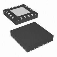
ISL6597CRZ Intersil, ISL6597CRZ Datasheet - Page 7

ISL6597CRZ
Manufacturer Part Number
ISL6597CRZ
Description
IC MOSFET DRVR DUAL SYNC 16-QFN
Manufacturer
Intersil
Datasheet
1.ISL6597CRZ.pdf
(10 pages)
Specifications of ISL6597CRZ
Configuration
High and Low Side, Synchronous
Input Type
Non-Inverting
Delay Time
18ns
Number Of Configurations
2
Number Of Outputs
4
High Side Voltage - Max (bootstrap)
36V
Voltage - Supply
4.5 V ~ 5.5 V
Operating Temperature
0°C ~ 70°C
Mounting Type
Surface Mount
Package / Case
16-VQFN Exposed Pad, 16-HVQFN, 16-SQFN, 16-DHVQFN
Lead Free Status / RoHS Status
Lead free / RoHS Compliant
Current - Peak
-
PWM line of ISL6597 (assuming an Intersil PWM controller
is used).
Bootstrap Considerations
This driver features an internal bootstrap diode. Simply
adding an external capacitor across the BOOT and PHASE
pins completes the bootstrap circuit.
The following equation helps select a proper bootstrap
capacitor size:
where Q
at V
control MOSFETs. The ΔV
allowable droop in the rail of the upper gate drive.
As an example, suppose two HAT2168 FETs are chosen as
the upper MOSFETs. The gate charge (Q
sheet is 12nC at 5V (V
Q
will assume a 100mV droop in drive voltage over the PWM
cycle. We find that a bootstrap capacitance of at least
0.264μF is required. The next larger standard value
capacitance is 0.33µF. A good quality ceramic capacitor is
recommended.
Power Dissipation
Package power dissipation is mainly a function of the
switching frequency (F
external gate resistance, and the selected MOSFET’s
internal gate resistance and total gate charge. Calculating
the power dissipation in the driver for a desired application is
critical to ensure safe operation. Exceeding the maximum
C
Q
GATE
BOOT_CAP
GATE
FIGURE 2. BOOTSTRAP CAPACITANCE vs BOOT RIPPLE
GS1
2.0
1.8
1.6
1.4
1.2
1.0
0.8
0.6
0.4
0.2
0.0
=
is calculated to be 26.4nC at 5.5V PVCC level. We
0.0
G1
gate-source voltage and N
Q
----------------------------------- - N
20nC
G1
is the amount of gate charge per upper MOSFET
≥
V
0.1
VOLTAGE
------------------------------------- -
ΔV
•
GS1
PVCC
BOOT_CAP
Q
0.2
GATE
50nC
Q
GATE
•
GS
SW
0.3
Q1
) gate-source voltage. Then the
), the output drive impedance, the
BOOT_CAP
= 100nC
ΔV
0.4
BOOT
7
0.5
(V)
Q1
0.6
term is defined as the
is the number of
G
0.7
) from the data
0.8
0.9
(EQ. 1)
1.0
ISL6597
allowable power dissipation level will push the IC beyond the
maximum recommended operating junction temperature of
+125°C. The maximum allowable IC power dissipation for
the 16 lead 4x4 QFN packages, with an exposed heat
escape pad, is around 2W. See Layout Considerations
paragraph for thermal transfer improvement suggestions.
When designing the driver into an application, it is
recommended that the following calculation is used to
ensure safe operation at the desired frequency for the
selected MOSFETs. The total gate drive power losses due to
the gate charge of MOSFETs and the driver’s internal
circuitry and their corresponding average driver current can
be estimated with Equations 2 and 3, respectively,
where the gate charge (Q
particular gate to source voltage (V
corresponding MOSFET datasheet; I
quiescent current with no load at both drive outputs; N
and N
respectively. The factor 2 is the number of active channels.
The I
without capacitive load and is typically negligible.
The total gate drive power losses are dissipated among the
resistive components along the transition path. The drive
resistance dissipates a portion of the total gate drive power
losses, the rest will be dissipated by the external gate
resistors (R
interfering with the operation shoot-through protection
circuitry) and the internal gate resistors (R
MOSFETs. Figures 3 and 4 show the typical upper and lower
gate drives turn-on transition path. The power dissipation on
the driver can be roughly estimated as:
P
P
P
R
I
P
DR
DR
DR_UP
DR_LOW
EXT2
Qg_TOT
P
P
=
Q
=
Qg_Q2
Qg_Q1
Q2
2
V
2
=
•
CC
=
are number of upper and lower MOSFETs,
•
R
⎛
⎜
⎝
=
=
(
Q
----------------------------- -
⎛
⎜
⎝
G1
G1
P
--------------------------------------
R
product is the quiescent power of the driver
=
⎛
⎜
⎝
2
G1
=
DR_UP
V
HI1
--------------------------------------
R
+
•
and R
Q
-------------------------------------- - F
Q
-------------------------------------- - F
GS1
HI2
(
•
R
-------------
R
N
G2
P
G1
+
N
GI1
HI1
R
Q1
Qg_Q1
Q1
R
+
V
V
HI2
•
•
+
GS2
EXT1
R
GS1
G2
PVCC
PVCC
P
+
EXT2
DR_LOW
Q
----------------------------- -
, should be a short to avoid
+
G2
G1
+
V
P
2
2
GS2
+
--------------------------------------- -
R
Qg_Q2
•
•
•
and Q
LO1
--------------------------------------- -
R
R
N
LO2
)
EXT2
Q2
SW
SW
R
+
+
LO1
R
I
⎞
⎟
⎠
)
Q
R
+
+
LO2
•
G2
GS1
•
•
•
EXT1
N
R
I
F
N
Q
=
Q
VCC
Q2
SW
) is defined at a
EXT2
Q1
R
•
and V
is the driver’s total
G2
VCC
⎞
⎟
⎠
+
GI1
•
⎞
⎟
⎠
I
+
Q
P
---------------------
•
GS2
R
-------------
N
Qg_Q1
P
---------------------
and R
GI2
Qg_Q2
Q2
2
2
) in the
May 4, 2007
GI2
(EQ. 3)
FN9165.1
(EQ. 2)
(EQ. 4)
Q1
) of


