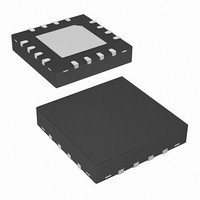
ISL6597CRZ Intersil, ISL6597CRZ Datasheet - Page 8

ISL6597CRZ
Manufacturer Part Number
ISL6597CRZ
Description
IC MOSFET DRVR DUAL SYNC 16-QFN
Manufacturer
Intersil
Datasheet
1.ISL6597CRZ.pdf
(10 pages)
Specifications of ISL6597CRZ
Configuration
High and Low Side, Synchronous
Input Type
Non-Inverting
Delay Time
18ns
Number Of Configurations
2
Number Of Outputs
4
High Side Voltage - Max (bootstrap)
36V
Voltage - Supply
4.5 V ~ 5.5 V
Operating Temperature
0°C ~ 70°C
Mounting Type
Surface Mount
Package / Case
16-VQFN Exposed Pad, 16-HVQFN, 16-SQFN, 16-DHVQFN
Lead Free Status / RoHS Status
Lead free / RoHS Compliant
Current - Peak
-
Application Information
MOSFET Selection
The parasitic inductances of the PCB and of the power
devices’ packaging (both upper and lower MOSFETs) can
cause serious ringing, exceeding absolute maximum rating
of the devices. The negative ringing at the edges of the
PHASE node could increase the bootstrap capacitor voltage
through the internal bootstrap diode, and in some cases, it
may overstress the upper MOSFET driver. Careful layout,
proper selection of MOSFETs and packaging can go a long
way toward minimizing such unwanted stress.
The D
parasitic lead inductances and are not recommended unless
a phase resistor (R
implemented to prevent the bootstrap capacitor from
FIGURE 4. TYPICAL LOWER-GATE DRIVE TURN-ON PATH
FIGURE 3. TYPICAL UPPER-GATE DRIVE TURN-ON PATH
FIGURE 5. PHASE RESISTOR TO MINIMIZE SERIOUS
PVCC
PVCC
2
PVCC
-PAK, or D-PAK packaged MOSFETs, have large
NEGATIVE PHASE SPIKE
R
R
LO2
R
HI2
R
R
R
LO1
LO1
HI1
HI1
PH
GND
LGATE
UGATE
UGATE
PHASE
PHASE
), as shown in Figure 5, is
BOOT
BOOT
R
8
G2
R
R
G
PH
G1
G
G
= 1Ω to 2Ω
R
C
GI2
GD
R
C
C
GI1
GD
GS
C
GS
S
S
S
D
D
D
Q1
Q2
C
Q1
DS
C
DS
ISL6597
overcharging, exceeding the device rating. Low-profile
MOSFETs, such as Direct FETs and multi-SOURCE leads
devices (SO-8, LFPAK, PowerPAK), have low parasitic lead
inductances and are preferred.
Layout Considerations
A good layout helps reduce the ringing on the switching
node (PHASE) and significantly lower the stress applied to
the output drives. The following advice is meant to lead to an
optimized layout and performance:
• Keep decoupling loops (VCC-GND, PVCC-PGND and
• Minimize trace inductance, especially on low-impedance
• Shorten all gate drive loops (UGATE-PHASE and LGATE-
• Minimize the inductance of the PHASE node. Ideally, the
• Minimize the current loop of the output and input power
• Avoid routing relatively high impedance nodes (such as
In addition, connecting the thermal pad of the QFN package
to the power ground through multiple vias is recommended.
This is to improve heat dissipation and allow the part to
achieve its full thermal potential.
Upper MOSFET Self Turn-On Effects At Startup
Should the driver have insufficient bias voltage applied, its
outputs are floating. If the input bus is energized at a high
dV/dt rate while the driver outputs are floating, due to the
self-coupling via the internal C
UGATE could momentarily rise up to a level greater than the
threshold voltage of the MOSFET. This could potentially turn
on the upper switch and result in damaging inrush energy.
Therefore, if such a situation (when input bus powered up
before the bias of the controller and driver is ready) could
conceivably be encountered, it is a common practice to
place a resistor (R
BOOT-PHASE) short and wide, at least 25 mils. Avoid
using vias on decoupling components other than their
ground terminals, which should be on a copper plane with
at least two vias.
lines. All power traces (UGATE, PHASE, LGATE, PGND,
PVCC, VCC, GND) should be short and wide, at least 25
mils. Try to place power traces on a single layer,
otherwise, two vias on interconnection are preferred
where possible. For no connection (NC) pins on the QFN
part, connect it to the adjacent net (LGATE2/PHASE2) can
reduce trace inductance.
PGND) and route them closely spaced.
source of the upper and the drain of the lower MOSFET
should be as close as thermally allowable.
trains. Short the source connection of the lower MOSFET
to ground as close to the transistor pin as feasible. Input
capacitors (especially ceramic decoupling) should be
placed as close to the drain of upper and source of lower
MOSFETs as possible.
PWM and ENABLE lines) close to high dV/dt UGATE and
PHASE nodes.
UGPH
) across the gate and source of the
GD
of the MOSFET, the
May 4, 2007
FN9165.1


