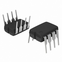
NCP5111PG ON Semiconductor, NCP5111PG Datasheet

NCP5111PG
Specifications of NCP5111PG
Available stocks
Related parts for NCP5111PG
NCP5111PG Summary of contents
Page 1
... Microdot may be in either location) PINOUT INFORMATION VCC GND 4 DRV_LO ORDERING INFORMATION Device Package NCP5111PG PDIP-8 (Pb-Free) NCP5111DR2G SOIC-8 (Pb-Free) †For information on tape and reel specifications, including part orientation and tape sizes, please refer to our Tape and Reel Packaging Specification Brochure, BRD8011/D. 1 MARKING DIAGRAMS ...
Page 2
Vbulk C1 D4 GND Vcc C3 U1 NCP5111 GND 1 Vcc 2 IN NCP1395 3 GND 4 DRV_LO GND GND Figure 1. Typical Application Resonant Converter (LLC type) + Vbulk C1 D4 GND Vcc C3 U1 NCP5111 GND 1 ...
Page 3
PIN DESCRIPTIONS Pin No. Pin Name 1 VCC Low side and main power supply 2 IN Logic Input 3 GND Ground 4 DRV_LO Low side gate drive output 5 NC Not Connected 6 BRIDGE Bootstrap return or high side floating ...
Page 4
ELECTRICAL CHARACTERISTIC (V Rating OUTPUT SECTION Output high short circuit pulsed current V DRV Output low short circuit pulsed current V DRV Output resistor (Typical value @ 25°C) Source Output resistor (Typical value @ 25°C) Sink High level output voltage, ...
Page 5
IN DRV_HI DRV_LO Note: DRV_HI output is in phase with the input. Figure 4. Input/Output Timing Diagram 50% IN ton Dead Time DRV_HI toff tf DRV_LO 90% 10% 50% IN Dead Time 1 DRV_HI toff_LO DRV_LO 90% NCP5111 50% tr ...
Page 6
T High Side ON 800 750 700 650 600 T ON 550 500 450 400 VOLTAGE (V) CC Figure 7. Turn ON Propagation Delay vs. Supply Voltage ( 140 ...
Page 7
High Side 120 r 100 Low Side VOLTAGE (V) CC Figure 13. Turn ON Risetime vs. Supply Voltage ( BOOT 80 ...
Page 8
V , VOLTAGE (V) CC Figure 19. Low Level Input Voltage Threshold vs. Supply Voltage (V 2.5 2 1 ...
Page 9
V , VOLTAGE (V) CC Figure 25. Logic “1” Input Current vs. Supply Voltage ( BOOT 1 0.8 0.6 0.4 0 ...
Page 10
I High Side 300 src 250 200 150 I Low Side src 100 VOLTAGE (V) CC Figure 31. Output Source Current vs. Supply Voltage ( BOOT 600 ...
Page 11
V , VOLTAGE (V) BOOT Figure 37. V Supply Current vs. Bootstrap BOOT Supply Voltage 240 200 160 120 VOLTAGE (V) ...
Page 12
nF LOAD GATE 0 0 100 200 300 400 SWITCHING FREQUENCY (kHz) Figure 43. I Consumption vs. Switching CC1 Frequency with 15 ...
Page 13
F -A- NOTE 2 C -T- N SEATING PLANE 0.13 (0.005) M NCP5111 PACKAGE DIMENSIONS 8 LEAD PDIP CASE 626-05 ISSUE http://onsemi.com ...
Page 14
... *For additional information on our Pb-Free strategy and soldering details, please download the ON Semiconductor Soldering and Mounting Techniques Reference Manual, SOLDERRM/D. The product described herein is covered by U.S. patents: 6,097,075; 7,176,723; 6,362,067. There may be some other patents pending. ON Semiconductor and are registered trademarks of Semiconductor Components Industries, LLC (SCILLC). SCILLC reserves the right to make changes without further notice to any products herein ...


