IR2130J International Rectifier, IR2130J Datasheet
IR2130J
Specifications of IR2130J
Available stocks


Related parts for IR2130J

IR2130J Summary of contents
Page 1
Features Floating channel designed for bootstrap operation Fully operational to +600V Tolerant to negative transient voltage dV/dt immune Gate drive supply range from 10 to 20V Undervoltage lockout for all channels Over-current shutdown turns off all six drivers Independent half-bridge ...
Page 2
IR2130/IR2132(J)(S) & (PbF) Absolute Maximum Ratings Absolute Maximum Ratings indicate sustained limits beyond which damage to the device may occur. All voltage param- eters are absolute voltages referenced to V under board mounted and still air conditions. Additional information is ...
Page 3
Dynamic Electrical Characteristics 15V, V BIAS CC BS1,2,3 S0,1,2,3 electrical characteristics are defined in Figures 3 through 5. Symbol Definition t Turn-On Propagation Delay on t Turn-Off Propagation Delay off t Turn-On Rise Time ...
Page 4
... SS A HIN1,2,3 Figure Min. Typ. Max. Units Test Conditions 38 200 39 420 40 — 41 — 5.0 45 — 46 2.3 47 1.0 48 — 49 — 44 Lead PLCC w/o 12 Leads IR2130J / IR2132J Part Number , V and I parameters & LIN1,2,3 . The V and I parameters O O 250 — 0V µs mA 500 — 15V, V ...
Page 5
Functional Block Diagram Lead Definitions Symbol Description HIN1,2,3 Logic inputs for high side gate driver outputs (HO1,2,3), out of phase LIN1,2,3 Logic inputs for low side gate driver output (LO1,2,3), out of phase FAULT Indicates over-current or undervoltage lockout (low ...
Page 6
IR2130/IR2132(J)(S) & (PbF) HIN1,2,3 LIN1,2,3 ITRIP FAULT HO1,2,3 LO1,2,3 Figure 1. Input/Output Timing Diagram HIN1,2,3 50% 50% LIN1,2,3 LO1,2,3 50% HO1,2,3 DT Figure 3. Deadtime Waveform Definitions 6 Figure 2. Floating Supply Voltage Transient Test Circuit HIN1,2,3 LIN1,2,3 50% t ...
Page 7
LIN1,2,3 50% ITRIP FAULT 50% LO1,2,3 50% t flt t itrip Figure 5. Overcurrent Shutdown Switching Time Waveform Definitions on HIN/LIN HO/LO www.irf.com IR2130/IR2132(J)(S) & (PbF) 50% 50% t fltclr t in,fil on on off off off high Figure 5.5 ...
Page 8
IR2130/IR2132(J)(S) & (PbF) 15V CA 90 SR Figure 7. Operational Amplifier Slew Rate Measurement 15V CA ...
Page 9
Max. 0.90 Typ. 0.60 Min. 0.30 0.00 -50 - Temperature (°C) Figure 11A. Turn-On Time vs. Temperature 1.50 Max 1.20 Typ. 0.90 0.60 0.30 0. Input Voltage (V) Figure 11C. Turn-On ...
Page 10
IR2130/IR2132(J)(S) & (PbF) 250 200 150 Max. 100 Typ -50 - Temperature (°C) Figure 13A. Turn-On Rise Time vs. Temperature 125 100 75 50 Max. Typ -50 - Temperature (°C) ...
Page 11
Max. 0.90 Typ. 0.60 Min. 0.30 0.00 -50 - Temperature (°C) FAULT Figure 16A. ITRIP to Indication Time vs. Temperature 25.0 20.0 15.0 Max. 10.0 Typ. Min. 5.0 0.0 -50 - Temperature ...
Page 12
IR2130/IR2132(J)(S) & (PbF) 2.50 2.00 1.50 Max. Typ. 1.00 Min. 0.50 0.00 -50 - Temperature (°C) Figure 18C. Deadtime vs. Temperature (IR2132) 10.0 8.0 Typ. 6.0 Min. 4.0 2.0 0.0 -50 - Temperature (°C) ...
Page 13
Min. 2.00 1.00 0.00 -50 - Temperature (°C) Figure 21A. Logic “0” Input Threshold vs. Temperature 5.00 4.00 3.00 2.00 1.00 Max. 0.00 -50 - Temperature (°C) Figure 22A. Logic “1” ...
Page 14
IR2130/IR2132(J)(S) & (PbF) 1.00 0.80 0.60 0.40 0.20 Max. 0.00 -50 - Temperature (°C) Figure 24A. High Level Output vs. Temperature 1.00 0.80 0.60 0.40 0.20 Max. 0.00 -50 - Temperature (°C) Figure 25A. ...
Page 15
Max. 20 Typ. 0 -50 - Temperature (°C) Figure 27A. V Supply Current vs. Temperature BS 10.0 8.0 6.0 4.0 Max. Typ. 2.0 0.0 -50 - Temperature (°C) Figure 28A. ...
Page 16
IR2130/IR2132(J)(S) & (PbF) 1.25 1.00 0.75 0.50 Max. 0.25 Typ. 0.00 -50 - Temperature (°C) Figure 30A. Logic “0” Input Current vs. Temperature 500 400 300 200 Max. 100 Typ. 0 -50 - Temperature ...
Page 17
Max. 9.0 Typ. 8.0 Min. 7.0 6.0 -50 - Temperature (°C) Figure 33. V Undervoltage (+) vs. Temperature BS 11.0 10.0 Max. 9.0 Typ. Min. 8.0 7.0 6.0 -50 - Temperature (°C) ...
Page 18
IR2130/IR2132(J)(S) & (PbF) 500 400 Typ. 300 Min. 200 100 0 -50 - Temperature (°C) Figure 38A. Output Source Current vs. Temperature 750 Typ. 600 Min. 450 300 150 0 -50 - Temperature (°C) ...
Page 19
Max. 4.0 2.0 0.0 -50 - Temperature (°C) Figure 41A. CA- Input Current vs. Temperature 100 80 Typ. 60 Min -50 - Temperature (°C) Figure 42A. Amplifier CMRR ...
Page 20
IR2130/IR2132(J)(S) & (PbF) 6.00 5.70 5.40 Max. Typ. 5.10 Min. 4.80 4.50 -50 - Temperature (°C) Figure 44A. Amplifier High Level Output vs. Temperature 100 Max -50 - Temperature ...
Page 21
Typ. 2.00 Min. 1.00 0.00 -50 - Temperature (°C) Figure 47A. Amplifier Output Sink Current vs. Temperature 15.0 12.0 9.0 Max. 6.0 Typ. 3.0 0.0 -50 - Temperature (°C) Figure 48A. ...
Page 22
IR2130/IR2132(J)(S) & (PbF) 0.0 -3.0 -6.0 -9.0 -12.0 -15.0 Figure 50. Maximum VS Negative Offset vs 1E+2 1E+3 1E+4 Frequency (Hz) Figure 51. IR2130/IR2132 T vs. Frequency (IRF820 ...
Page 23
... GATE CC www.irf.com IR2130/IR2132(J)(S) & (PbF 480V 4 0 320V 160V 1E Figure 56. IR2130J/IR2132J T vs. Frequency (IRGPC30KD2 GATE 120 110 100 480V 50 320V 40 160V 1E+5 1E+2 1E+3 Figure 58. IR2130J/IR2132J T vs. Frequency (IRGPC50KD2 GATE Frequency (Hz 15V CC 480V 320V 160V 0V 1E+4 1E+5 Frequency (Hz) = 15V CC 23 ...
Page 24
IR2130/IR2132(J)(S) & (PbF) Case outlines 24 28-Lead PDIP (wide body) 28-Lead SOIC (wide body) 01-6011 01-3024 02 (MS-011AB 01-304002 (MS-013AE) www.irf.com ...
Page 25
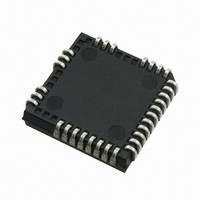
Case outline 44-Lead PLCC w/o 12 leads www.irf.com IR2130/IR2132(J)(S) & (PbF) NOTES 01-6009 00 01-3004 02(mod. ) (MS-018AC) 25 ...
Page 26
... PDIP IR2130 order IR2130PbF 28-Lead SOIC IR2130S order IR2130SPbF 28-Lead PDIP IR2132 order IR2132PbF 28-Lead SOIC IR2132S order IR2132SPbF 44-Lead PLCC IR2130J order IR2130JPbF 44-Lead PLCC IR2132J order IR2132JPbF This product has been qualified per industrial level Data and specifications subject to change without notice. ...