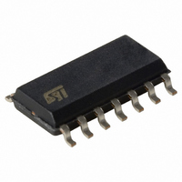
L6386D013TR STMicroelectronics, L6386D013TR Datasheet - Page 5

L6386D013TR
Manufacturer Part Number
L6386D013TR
Description
IC DRIVER HI/LO SIDE HV 14-SOIC
Manufacturer
STMicroelectronics
Type
Driverr
Datasheet
1.L6386D.pdf
(10 pages)
Specifications of L6386D013TR
Configuration
High and Low Side, Independent
Input Type
Non-Inverting
Delay Time
110ns
Current - Peak
400mA
Number Of Configurations
1
Number Of Outputs
2
High Side Voltage - Max (bootstrap)
600V
Voltage - Supply
17V
Operating Temperature
-40°C ~ 125°C
Mounting Type
Surface Mount
Package / Case
8-SOIC (3.9mm Width)
Product
H-Bridge Drivers
Rise Time
50 ns
Fall Time
30 ns
Supply Voltage (min)
8 V
Supply Current
0.32 mA
Maximum Power Dissipation
750 mW
Maximum Operating Temperature
+ 125 C
Mounting Style
SMD/SMT
Minimum Operating Temperature
- 45 C
Number Of Drivers
2
For Use With
497-5492 - EVAL BOARD FOR L6384/L6385/L6386
Lead Free Status / RoHS Status
Lead free / RoHS Compliant
Other names
497-3651-2
Available stocks
Company
Part Number
Manufacturer
Quantity
Price
Part Number:
L6386D013TR
Manufacturer:
ST
Quantity:
20 000
BOOTSTRAP DRIVER
A bootstrap circuitry is needed to supply the high
voltage section. This function is normally accom-
plished by a high voltage fast recovery diode (fig.
4a). In the L6386 a patented integrated structure
replaces the external diode. It is realized by a
high voltage DMOS, driven synchronously with
the low side driver (LVG), with in series a diode,
as shown in fig. 4b
An internal charge pump (fig. 4b) provides the
DMOS driving voltage .
The diode connected in series to the DMOS has
been added to avoid undesirable turn on of it.
CBOOT selection and charging:
To choose the proper C
MOS can be seen as an equivalent capacitor.
This capacitor C
gate charge :
The ratio between the capacitors C
is proportional to the cyclical voltage loss .
It has to be:
e.g.: if Q
3nF. With
300mV.
If HVG has to be supplied for a long time, the
C
leakage losses.
e.g.: HVG steady state consumption is lower than
200 A, so if HVG T
Figure 4. Bootstrap Driver.
BOOT
V
selection has to take into account also the
S
gate
C
BOOT
is 30nC and V
D
BOOT
C
EXT
BOOT
C
= 100nF the drop would be
EXT
a
is related to the MOS total
ON
HVG
LVG
>>>C
BOOT
is 5ms, C
Q
V
gate
gate
EXT
gate
value the external
is 10V, C
V
V
EXT
BOOT
OUT
BOOT
H.V.
and C
has to
EXT
C
BOOT
TO LOAD
BOOT
is
V
supply 1 C to C
pacitor means a voltage drop of 1V.
The internal bootstrap driver gives great advan-
tages: the external fast recovery diode can be
avoided (it usually has great leakage current).
This structure can work only if V
GND (or lower) and in the meanwhile the LVG is
on. The charging time (T
Ohm). At low frequency this drop can be ne-
glected. Anyway
must be taken in to account.
The following equation is useful to compute the
drop on the bootstrap DMOS:
the time in which both conditions are fulfilled and
it has to be long enough to charge the capacitor.
The bootstrap driver introduces a voltage drop
due to
where Q
power MOS, R
bootstrap DMOS, and T
of the bootstrap capacitor.
For example: using a power MOS with a total
gate charge of 30nC the drop on the bootstrap
DMOS is about 1V, if the T
V
age drop on C
too high, or the circuit topology doesn’t allow a
sufficient charging time, an external diode can be
used.
S
drop
V
has to be taken into account when the volt-
drop
gate
the DMOS R
V
I
charge
drop
is the gate charge of the external
b
BOOT
HVG
LVG
dson
R
EXT
30nC
dson
5 s
increasing the frequency
. This charge on a 1 F ca-
is the on resistance of the
is calculated: if this drop is
DSON
charge
charge
125
V
charge
drop
V
V
BOOT
OUT
(typical value: 125
is the charging time
H.V.
) of the C
~
T
is 5 s. In fact:
0.8V
OUT
Q
charge
gate
D99IN1056
C
TO LOAD
is close to
BOOT
R
dson
BOOT
L6386
5/10
is
it


