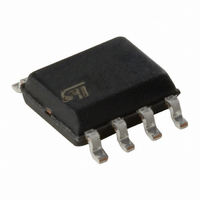
L6387D STMicroelectronics, L6387D Datasheet

L6387D
Specifications of L6387D
L6387D
Available stocks
Related parts for L6387D
L6387D Summary of contents
Page 1
... IGBT. The Upper (Floating) Section is enabled to work with voltage Rail up to 600V. The Logic In- puts are CMOS/TTL compatible for ease of inter- facing with controlling devices LEVEL LOGIC SHIFTER LVG DRIVER L6387 Minidip ORDERING NUMBERS: L6387D L6387 8 Vboot H.V. HVG DRIVER HVG 7 OUT 6 TO LOAD V CC ...
Page 2
L6387 ABSOLUTE MAXIMUM RATINGS Symbol Vout Output Voltage Vcc Supply Voltage Vboot Floating Supply Voltage Vhvg Upper Gate Output Voltage Vlvg Lower Gate Output Voltage Vi Logic Input Voltage dVout/dt Allowed Output Slew Rate Ptot Total Power Dissipation (Tj = ...
Page 3
RECOMMENDED OPERATING CONDITIONS Symbol Pin Parameter Vout 6 Output Voltage Vboot- 8 Floating Supply Voltage Vout fsw Switching Frequency Vcc 2 Supply Voltage T Junction Temperature j Note 1: If the condition Vboot - Vout < 18V is guaranteed, Vout ...
Page 4
L6387 Figure 1. Typical Rise and Fall Times vs. Load Capacitance time (nsec) 250 200 150 100 For both high and low side buffers @25˚C Tamb Input Logic L6387 Input Logic is V (17V) ...
Page 5
DMOS drop charge dson drop where Q is the gate charge of the external gate power MOS the on resistance of the dson bootstrap DMOS, and T charge of the ...
Page 6
L6387 Figure 6. Output Source Current vs. Temperature 1000 800 600 Typ. 400 200 0 -45 - (°C) 6/9 Figure 7. Output Sink Current vs. Temperature 1000 @ Vcc = 15V 800 600 400 200 50 75 ...
Page 7
DIM. MIN. TYP. MAX. MIN. A 3.32 a1 0.51 0.020 B 1.15 1.65 0.045 b 0.356 0.55 0.014 b1 0.204 0.304 0.008 D 10.92 E 7.95 9.75 0.313 e 2.54 e3 7.62 e4 7.62 F 6.6 I 5.08 L ...
Page 8
L6387 mm DIM. MIN. TYP. MAX. MIN. A 1.75 a1 0.1 0.25 0.004 a2 1.65 a3 0.65 0.85 0.026 b 0.35 0.48 0.014 b1 0.19 0.25 0.007 C 0.25 0.5 0.010 c1 45 (typ.) D (1) 4.8 5.0 0.189 E ...
Page 9
... STMicroelectronics. Specification mentioned in this publication are subject to change without notice. This publication supersedes and replaces all information previously supplied. STMicroelectronics products are not authorized for use as critical components in life support devices or systems without express written approval of STMicroelectronics. The ST logo is a registered trademark of STMicroelectronics © ...


