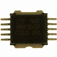
VND830ASP13TR STMicroelectronics, VND830ASP13TR Datasheet

VND830ASP13TR
Specifications of VND830ASP13TR
Available stocks
Related parts for VND830ASP13TR
VND830ASP13TR Summary of contents
Page 1
... OVERVOLTAGE UNDERVOLTAGE PwCLAMP 1 DRIVER 1 I LIM1 V dslim1 LOGIC I OUT1 K PwCLAMP 2 DRIVER 2 Ot1 I LIM2 V dslim2 I Ot2 OUT2 K VND830ASP 10 1 PowerSO-10™ ORDER CODES TUBE T&R VND830ASP VND830ASP13TR pin voltage OUTPUT 1 Ot1 CURRENT SENSE 1 OUTPUT 2 Ot2 CURRENT SENSE 2 1/17 ...
Page 2
VND830ASP ABSOLUTE MAXIMUM RATING Symbol V DC Supply Voltage CC -V Reverse Supply Voltage Reverse Ground Pin Current GND I Output Current OUT I Reverse Output Current R I Input Current IN V Current Sense Maximum Voltage ...
Page 3
THERMAL DATA Symbol R Thermal Resistance Junction-case thj-case R Thermal Resistance Junction-ambient thj-amb (*) When mounted on a standard single-sided FR-4 board with 0.5cm flow ELECTRICAL CHARACTERISTICS (8V<V (Per each channel) POWER OUTPUT Symbol Parameter V Operating Supply Voltage CC ...
Page 4
VND830ASP ELECTRICAL CHARACTERISTICS (continued OUTPUT DIODE CC Symbol Parameter V Forward on Voltage F PROTECTIONS Symbol Parameter I Current limitation lim Thermal shut-down T TSD temperature T Thermal reset temperature R T Thermal hysteresis HYST V Turn-off output ...
Page 5
TRUTH TABLE (per channel) CONDITIONS Normal operation Overtemperature Undervoltage Overvoltage Short circuit to GND Short circuit Negative output voltage clamp ELECTRICAL TRANSIENT REQUIREMENTS ISO T/R 7637/1 I Test Pulse -25 ...
Page 6
VND830ASP Figure versus I OUT SENSE OUT Iout/Isense 2250 2000 1750 1500 1250 1000 750 500 0 Figure 2: Switching Characteristics (Resistive load R V OUT 80% dV /dt OUT (on) I SENSE 90% t DSENSE INPUT ...
Page 7
Figure 3: Waveforms INPUT n LOAD CURRENT n SENSE USD INPUT n LOAD CURRENT n SENSE INPUT n LOAD CURRENT n SENSE n INPUT n LOAD CURRENT n LOAD VOLTAGE ...
Page 8
VND830ASP APPLICATION SCHEMATIC +5V R prot R prot C R prot R prot R R SENSE1 GND PROTECTION NETWORK REVERSE BATTERY Solution 1: Resistor in the ground line (R can be used with any type of load. The following is ...
Page 9
C I/Os PROTECTION ground protection network is used and negative transient are present on the V line, the control pins will CC be pulled negative. ST suggests to insert a resistor (R in line to prevent the C ...
Page 10
VND830ASP Off State Output Current IL(off1) (uA Off state 6 Vcc=13V Vin=Vout= -50 - 100 Tc (ºC) Input Clamp Voltage Vicl (V) 8 7.8 Iin=1mA 7.6 7.4 7.2 ...
Page 11
Overvoltage Shutdown Vov (V) 50 47.5 45 42.5 40 37.5 35 32.5 30 -50 - 100 Tc (ºC) Turn-on Voltage Slope dVout/dt(on) (V/ms) 600 550 Vcc=13V Rl=6.5Ohm 500 450 400 350 300 250 200 -50 -25 ...
Page 12
VND830ASP Maximum turn off current versus load inductance I LMAX (A) 100 Single Pulse at T =150ºC Jstart B= Repetitive pulse at T =100ºC Jstart C= Repetitive Pulse at T =125ºC Jstart Conditions: V =13.5V ...
Page 13
PowerSO-10™ THERMAL DATA PowerSO-10™ PC Board Layout condition of R and thickness=35 m, Copper areas: from minimum pad lay-out to 8cm R Vs PCB copper area in open box free air condition thj-amb RTHj_amb (°C/ ...
Page 14
VND830ASP PowerSO-10 Thermal Impedance Junction Ambient Single Pulse ZTH (°C/W) 1000 100 10 1 0.1 0.0001 0.001 0.01 Thermal fitting model of a double channel HSD in PowerSO-10 Tj_1 Pd1 C1 C2 ...
Page 15
PowerSO-10™ MECHANICAL DATA DIM. MIN. A 3.35 A (*) 3.4 A1 0.00 B 0.40 B (*) 0.37 C 0.35 C (*) 0.23 D 9.40 D1 7.40 E 9.30 E2 7.20 E2 (*) 7.30 E4 5.90 E4 (*) 5. ...
Page 16
VND830ASP SUGGESTED PAD LAYOUT PowerSO-10™ 14.6 - 14 TAPE AND REEL SHIPMENT (suffix “13TR”) TAPE DIMENSIONS According to Electronic Industries Association (EIA) Standard 481 rev. ...
Page 17
... STMicroelectronics. Specifications mentioned in this publication are subject to change without notice. This publication supersedes and replaces all information previously supplied. STMicroelectronics products are not authorized for use as critical components in life support devices or systems without express written approval of STMicroelectronics. 2003 STMicroelectronics - Printed in ITALY- All Rights Reserved. ...


