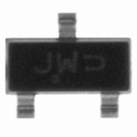
MDC3105LT1G ON Semiconductor, MDC3105LT1G Datasheet

MDC3105LT1G
Specifications of MDC3105LT1G
MDC3105LT1GOS
MDC3105LT1GOSTR
Available stocks
Related parts for MDC3105LT1G
MDC3105LT1G Summary of contents
Page 1
MDC3105 Integrated Relay, Inductive Load Driver This device is intended to replace an array of three to six discrete components with an integrated SMT part available in a SOT−23 package. It can be used to switch 3 to ...
Page 2
V out GND CASE 318 MAXIMUM RATINGS (T = 25°C unless otherwise noted) J Rating Power Supply Voltage Input Voltage Reverse Input Voltage Repetitive Pulse Zener ...
Page 3
... Output Sink Current − Continuous (V = 0.25 Vdc 1.5 mA ORDERING INFORMATION Device MDC3105LT1 MDC3105LT1G MDC3105DMT1 MDC3105DMT1G MDC3105XV6T1G †For information on tape and reel specifications, including part orientation and tape sizes, please refer to our Tape and Reel Packaging Specifications Brochure, BRD8011/ 25°C unless otherwise noted) A ≤ ...
Page 4
TYPICAL APPLICATION−DEPENDENT SWITCHING PERFORMANCE SWITCHING CHARACTERISTICS Characteristic Propagation Delay Times: High to Low Propagation Delay; Figure 1 (5.0 V 74HC04) Low to High Propagation Delay; Figure 1 (5.0 V 74HC04) High to Low Propagation Delay; Figures 1, 13 (3.0 V ...
Page 5
TYPICAL PERFORMANCE CHARACTERISTICS 500 450 T = 85°C J 400 25°C 350 300 250 -40°C 200 150 100 50 0 1.0 10 100 I , OUTPUT SINK CURRENT (mA) O Figure 2. Transistor DC Current Gain ...
Page 6
TYPICAL PERFORMANCE CHARACTERISTICS 10,000 5.5 Vdc CC 1000 k 100 1.0 k 100 10 1.0 -55 -35 -15 5 JUNCTION TEMPERATURE (°C) J Figure 8. Output Leakage Current versus Temperature 1.0 ...
Page 7
Figure 11. Zener Repetitive Pulse Energy Limit 1 0.5 0.2 0.1 0.1 0.05 0.02 0.01 0.01 SINGLE PULSE 0.001 0.01 0.1 1.0 Figure 12. Transient Thermal Response for MDC3105LT1 ...
Page 8
Using TTR Designing for Pulsed Operation For a repetitive pulse operating condition, time averaging allows one to increase a device’s peak power dissipation rating above the average rating by dividing by the duty cycle of the repetitive pulse train. Thus, ...
Page 9
Designing with this Data Sheet 1. Determine the maximum inductive load current (at max V , min coil resistance and usually minimum CC temperature) that the MDC3105 will have to drive and make sure it is less than the max ...
Page 10
Max Continuous Current Calculation for TX2−5V Relay 178 W Nominal @ R Assuming ±10% Make Tolerance 178 W * 0.9 = 160 W Min @ T = 25° for Annealed Copper Wire is 0.4%/°C ...
Page 11
TIME (ms) Figure 16 Square Wave Input TIME (ms) Figure 18 Square Wave Response TYPICAL OPERATING WAVEFORMS 225 175 ...
Page 12
... *For additional information on our Pb−Free strategy and soldering details, please download the ON Semiconductor Soldering and Mounting Techniques Reference Manual, SOLDERRM/D. PACKAGE DIMENSIONS SOT−23 (TO−236) CASE 318−08 ISSUE AN NOTES: 1. DIMENSIONING AND TOLERANCING PER ANSI Y14.5M, 1982. 2. CONTROLLING DIMENSION: INCH. 3. MAXIMUM LEAD THICKNESS INCLUDES LEAD FINISH THICKNESS ...
Page 13
... SOLDERING FOOTPRINT* 1.9 0.074 0.7 0.028 1.0 0.039 *For additional information on our Pb−Free strategy and soldering details, please download the ON Semiconductor Soldering and Mounting Techniques Reference Manual, SOLDERRM/D. PACKAGE DIMENSIONS SC−74 CASE 318F−05 ISSUE M NOTES: 1. DIMENSIONING AND TOLERANCING PER ANSI Y14.5M, 1982. ...
Page 14
... Pb−Free strategy and soldering details, please download the ON Semiconductor Soldering and Mounting Techniques Reference Manual, SOLDERRM/D. ON Semiconductor and are registered trademarks of Semiconductor Components Industries, LLC (SCILLC). SCILLC reserves the right to make changes without further notice to any products herein ...


