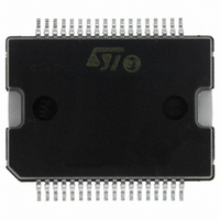
L6207PD013TR STMicroelectronics, L6207PD013TR Datasheet

L6207PD013TR
Specifications of L6207PD013TR
497-4575-2
497-4575-2
E-L6207PD013TR
Available stocks
Related parts for L6207PD013TR
L6207PD013TR Summary of contents
Page 1
OPERATING SUPPLY VOLTAGE FROM 8 TO 52V 5.6A OUTPUT PEAK CURRENT (2.8A DC) R 0.3 TYP. VALUE @ T DS(ON) OPERATING FREQUENCY UP TO 100KHz NON DISSIPATIVE OVERCURRENT PROTECTION DUAL INDEPENDENT CONSTANT t CURRENT CONTROLLERS SLOW DECAY SYNCHRONOUS RECTIFICATION CROSS ...
Page 2
L6207 ABSOLUTE MAXIMUM RATINGS Symbol Parameter V Supply Voltage S V Differential Voltage between OUT1 , OUT2 , SENSE OUT1 , OUT2 Bootstrap Peak Voltage BOOT V ,V Input ...
Page 3
THERMAL DATA Symbol R Maximum Thermal Resistance Junction-Pins th-j-pins R Maximum Thermal Resistance Junction-Case th-j-case R th-j-amb1 Maximum Thermal Resistance Junction-Ambient R th-j-amb1 Maximum Thermal Resistance Junction-Ambient R th-j-amb1 Maximum Thermal Resistance Junction-Ambient R th-j-amb2 Maximum Thermal Resistance Junction-Ambient (1) ...
Page 4
L6207 PIN DESCRIPTION PACKAGE SO24/ PowerSO36 Name PowerDIP24 PIN # PIN # 1 10 IN1 2 11 IN2 3 12 SENSE OUT1 18, GND 18 OUT1 9 ...
Page 5
PIN DESCRIPTION (continued VREF (6) Also connected at the output drain of the Over current and Thermal protection MOSFET. Therefore, it has to be driven putting in series a resistor with a value in the ...
Page 6
L6207 ELECTRICAL CHARACTERISTICS (continued ° 48V, unless otherwise specified) amb s Symbol Parameter Switching Characteristics t Enable to out turn ON delay time D(on)EN t Input to out turn ON delay time D(on)IN t (8) ...
Page 7
Figure 1. Switching Characteristic Definition EN V th(ON) V th(OFF) I OUT 90% 10% D01IN1316 Figure 2. Overcurrent Detection Timing Definition I OUT I SOVER ON BRIDGE OFF V EN 90% 10% t FALL t t D(OFF)EN D(ON) ...
Page 8
L6207 CIRCUIT DESCRIPTION POWER STAGES and CHARGE PUMP The L6207 integrates two independent Power MOS Full Bridges. Each Power MOS has an Rdson = 0.3ohm (typical value @ 25°C), with intrinsic fast freewheeling diode. Cross conduction protection is achieved using ...
Page 9
TRUTH TABLE INPUTS EN IN1 IN2 Don't care High Z = High Impedance Output GND (Vs) = GND during Ton, Vs during Toff ...
Page 10
L6207 Figure 8. Output Current Regulation Waveforms I OUT V REF R SENSE V SENSE V REF 2.5V ON SYNCHRONOUS RECTIFICATION OFF D02IN1351 Figure 9 shows the magnitude of the Off Time t culated from the ...
Page 11
PWM stage. Furthermore, the on time t RCRISE can not be smaller than the minimum on time t t > 1.5 s (typ. value ...
Page 12
L6207 Figure 10. Area where t can vary maintaining the PWM regulation. ON 100 10 1 0.1 SLOW DECAY MODE Figure 11 shows the operation of the bridge in the Slow Decay mode. At the start of the off time, ...
Page 13
NON-DISSIPATIVE OVERCURRENT PROTECTION The L6207 integrates an Overcurrent Detection Circuit (OCD). This circuit provides protection against a short circuit to ground or between two phases of the bridge. With this internal over current detection, the external cur- rent sense resistor ...
Page 14
L6207 Figure 13. Overcurrent Protection Waveforms I OUT I SOVER th(ON) V th(OFF) ON OCD OFF ON BRIDGE OFF t OCD(ON) 14/23 V EN(LOW DELAY EN(FALL) OCD(OFF) t D(OFF)EN DISABLE ...
Page 15
Figure 14. t versus C DISABLE Figure 15. t versus C DELAY 0.1 1 THERMAL PROTECTION In ...
Page 16
L6207 APPLICATION INFORMATION A typical application using L6207 is shown in Fig. 16. Typical component values for the application are shown in Table 3. A high quality ceramic capacitor in the range of 100 to 200 nF should be placed ...
Page 17
OUTPUT CURRENT CAPABILITY AND IC POWER DISSIPATION In Fig. 17 and Fig. 18 are shown the approximate relation between the output current and the IC power dissipa- tion using PWM current control driving two loads, for two different driving types: ...
Page 18
L6207 Figure 19. Mounting the PowerSO package. Slug soldered to PCB with dissipating area Figure 20. PowerSO36 Junction-Ambient thermal resistance versus on-board copper area. º Figure ...
Page 19
Figure 23. Typical Quiescent Current vs. Supply Voltage 5 1kHz sw 5.4 5.2 5.0 4.8 4 [V] S Figure 24. Normalized Typical Quiescent Current vs. Switching Frequency Iq / (Iq ...
Page 20
L6207 mm DIM. MIN. TYP. MAX. A 3.60 a1 0.10 0.30 0.004 a2 3. 0.10 b 0.22 0.38 0.008 c 0.23 0.32 0.009 D (1) 15.80 16.00 0.622 D1 9.40 9.80 0.370 E 13.90 14.50 0.547 e 0.65 ...
Page 21
DIM. MIN. TYP. MAX. MIN. A 4.320 A1 0.380 0.015 A2 3.300 B 0.410 0.460 0.510 0.016 B1 1.400 1.520 1.650 0.055 c 0.200 0.250 0.300 0.008 D 31.62 31.75 31.88 1.245 E 7.620 8.260 0.300 e 2.54 E1 ...
Page 22
L6207 mm DIM. MIN. TYP. MAX. A 2.35 2.65 0.093 A1 0.10 0.30 0.004 B 0.33 0.51 0.013 C 0.23 0.32 0.009 15.20 15.60 0.598 ( 7.40 7.60 0.291 e 1.27 H 10.0 10.65 0.394 h 0.25 0;75 ...
Page 23
... No license is granted by implication or otherwise under any patent or patent rights of STMicroelectronics. Specifications mentioned in this publication are subject to change without notice. This publication supersedes and replaces all information previously supplied. STMicroelectronics products are not authorized for use as critical components in life support devices or systems without express written approval of STMicroelectronics ...


