MAX4821ETP+ Maxim Integrated Products, MAX4821ETP+ Datasheet
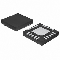
IC RELAY DRIVER 8CHAN 20-TQFN

MAX4821ETP+

Manufacturer Part Number
MAX4821ETP+
Description
IC RELAY DRIVER 8CHAN 20-TQFN
Manufacturer
Maxim Integrated Products
Type
Relay/Lamp Driverr
Datasheet

Specifications of MAX4821ETP+

Input Type
Parallel/Serial
Number Of Outputs
8
On-state Resistance
2 Ohm
Current - Output / Channel
70mA
Current - Peak Output
150mA
Voltage - Supply
2.3 V ~ 5.5 V
Operating Temperature
-40°C ~ 85°C
Mounting Type
Surface Mount
Package / Case
20-TQFN Exposed Pad
Lead Free Status / RoHS Status
Lead free / RoHS Compliant
The MAX4820/MAX4821 8-channel relay drivers offer
built-in kickback protection and drive +3.3V/+5V non-
latching or dual-coil-latching relays. These devices are
especially useful when driving +3V relays. Each inde-
pendent open-drain output features a 2Ω on-resistance
and is guaranteed to sink 70mA (min) of load current.
Both devices consume less than 50µA (max) quiescent
current and have 1µA output off-leakage current.
The MAX4820 features an SPI™-/QSPI™-/MICROWIRE™-
compatible serial interface. Input data is shifted into an 8-
bit shift register and latched to the outputs when CS
transitions from low to high. Each data bit in the shift reg-
ister corresponds to a specific output, allowing indepen-
dent control of all outputs.
The MAX4821 features a 4-bit (A0, A1, A2, LVL) paral-
lel-input interface. The first three bits (A0, A1, A2) deter-
mine the output address, and the fourth bit (LVL)
determines whether the selected output is switched on
or off. Data is latched to the outputs when CS transi-
tions from low to high.
Both devices feature separate set and reset functions
that allow the user to turn on or turn off all outputs simul-
taneously with a single control line. Built-in hysteresis
(Schmidt trigger) on all digital inputs allows this device
to be used with slow rising and falling signals, such as
those from optocouplers or RC power-up initialization
circuits. The MAX4820/MAX4821 are available in 20-pin
TSSOP and space-saving 20-pin Thin QFN packages.
19-2751; Rev 2; 1/10
Pin Configurations continued at end of data sheet.
Typical Application Circuits and Functional Diagrams
appear at end of data sheet.
SPI and QSPI are trademarks of Motorola, Inc.
MICROWIRE is a trademark of National Semiconductor Corp.
For pricing, delivery, and ordering information, please contact Maxim Direct at 1-888-629-4642,
or visit Maxim’s website at www.maxim-ic.com.
+3.3V/+5V, 8-Channel, Cascadable Relay Drivers
Central Office
ATE
DSL, ADSL Line Cards
Industrial Equipment
E1/T1 Redundancy
________________________________________________________________ Maxim Integrated Products
General Description
Applications
with Serial/Parallel Interface
♦ 8 Independent Output Channels
♦ Built-In Inductive Kickback Protection
♦ Drive +3V and +5V Relays
♦ Guaranteed 70mA (min) Coil Drive Current
♦ SET Function to Turn On All Outputs
♦ RESET Function to Turn Off All Outputs
♦ SPI-/QSPI-/MICROWIRE-Compatible Serial
♦ Serial Digital Output for Daisy Chaining
♦ Parallel Interface (MAX4821)
♦ Low 50µA (max) Quiescent Supply Current
♦ Space-Saving 20-Pin Thin QFN Package
+ Denotes a lead(Pb)-free/RoHS-compliant package.
* EP = Exposed pad.
MAX4820ETP+
MAX4820EUP+
MAX4821ETP+
MAX4821EUP+
Simultaneously
Simultaneously
Interface (MAX4820)
(MAX4820)
TOP VIEW
*CONNECT EP TO GND.
PART
RESET
DOUT
SCLK
DIN
CS
1
2
3
4
5
+
-40°C to +85°C
-40°C to +85°C
-40°C to +85°C
-40°C to +85°C
TEMP RANGE
*EP
Ordering Information
THIN QFN
MAX4820
Pin Configurations
PIN-PACKAGE
20 Thin QFN-EP*
20 TSSOP-EP*
20 Thin QFN-EP*
20 TSSOP-EP*
15
14
13
12
11
Features
OUT3
OUT4
COM
OUT5
OUT6
1

Related parts for MAX4821ETP+

MAX4821ETP+ Summary of contents

Page 1

... Low 50µA (max) Quiescent Supply Current ♦ Space-Saving 20-Pin Thin QFN Package PART TEMP RANGE MAX4820ETP+ -40°C to +85°C MAX4820EUP+ -40°C to +85°C MAX4821ETP+ -40°C to +85°C MAX4821EUP+ -40°C to +85°C + Denotes a lead(Pb)-free/RoHS-compliant package Exposed pad. TOP VIEW + RESET ...

Page 2

Cascadable Relay Drivers with Serial/Parallel Interface ABSOLUTE MAXIMUM RATINGS (All voltages referenced to GND COM..............................................................-0.3V to +6.0V CC OUT_........................................................-0. CS, SCLK, DIN, SET, RESET, A0, A1, A2, LVL......-0.3V to +6.0V DOUT..........................................................-0. Continuous ...

Page 3

Cascadable Relay Drivers ELECTRICAL CHARACTERISTICS (continued +3V to +5.5V -40°C to +85°C, unless otherwise noted. Typical values are COM CC A PARAMETER SYMBOL SPI TIMING (MAX4820) Turn-On ...

Page 4

Cascadable Relay Drivers with Serial/Parallel Interface ( -40°C to +85°C, unless otherwise noted. Typical values are at T COM CC A SUPPLY CURRENT vs. SUPPLY VOLTAGE 25 ALL LOGIC INPUTS = 0 20 ...

Page 5

Cascadable Relay Drivers ( -40°C to +85°C, unless otherwise noted. Typical values are at T COM CC A INPUT LOGIC THRESHOLD vs. SUPPLY VOLTAGE 2.50 2.25 2.00 1.75 1.50 1.25 1.00 0.75 0.50 ...

Page 6

Cascadable Relay Drivers with Serial/Parallel Interface PIN MAX4820 MAX4821 THIN THIN TSSOP TSSOP QFN QFN ...

Page 7

Cascadable Relay Drivers CS t CSS SCLK DIN D7 DOUT OUT_ Figure 1. 3-Wire Serial-Interface Timing Diagram (MAX4820 only) Table 1. Serial Input Address Map (MAX4820 Only) DIN D0 D1 OUT_ OUT1 OUT2 Serial ...

Page 8

Cascadable Relay Drivers with Serial/Parallel Interface LVL V OUT Figure 2. Parallel Interface Timing Diagram (MAX4821 only 0.1μ DIN DIN DOUT MAX4820 OUT1 SCLK SCLK OUT8 CS GND PGND CS ...

Page 9

Cascadable Relay Drivers is shifted through all the MAX4820s in series. When CS goes high, all outputs update simultaneously. The MAX4820 can also be used in a slave configuration that allows the user to address individual devices. Connect ...

Page 10

Cascadable Relay Drivers with Serial/Parallel Interface V CC RESET SET DIN DOUT SCLK RESET SET LVL ______________________________________________________________________________________ COM MAX4820 PARALLEL REGISTER 8-BIT SHIFT REGISTER PGND GND COM MAX4821 PARALLEL LATCH ...

Page 11

Cascadable Relay Drivers TOP VIEW + RESET LVL 3 MAX4821 THIN QFN *CONNECT EP TO GND. Chip Information PROCESS: BiCMOS ______________________________________________________________________________________ with Serial/Parallel Interface Pin Configurations (continued ...

Page 12

... Maxim cannot assume responsibility for use of any circuitry other than circuitry entirely embodied in a Maxim product. No circuit patent licenses are implied. Maxim reserves the right to change the circuitry and specifications without notice at any time. 12 ____________________Maxim Integrated Products, 120 San Gabriel Drive, Sunnyvale, CA 94086 408-737-7600 © 2010 Maxim Integrated Products ...

Related keywords