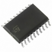
L9333MD STMicroelectronics, L9333MD Datasheet

L9333MD
Specifications of L9333MD
Available stocks
Related parts for L9333MD
L9333MD Summary of contents
Page 1
... VOLTAGE DESCRIPTION The L9333 is a monolithic integrated quad low side driver intended to drive lines, lamps or relais in > 45V FB automotive or industrial applications. CHANNEL & TIC REF ERE NCE L9333 SO20 (12+4+4) DIE ORDERING NUMBERS: L9333MD (SO20 12+4+4) L9333DIE1 (DIE IAG V int 1/13 ...
Page 2
L9333 PIN CONNECTION (Top view) PIN FUNCTION Pin Pin Name N° Input Input 2 3 DIAG Diagnostic GND Ground 14, 15, 16 Supply Voltage 9 IN ...
Page 3
ABSOLUTE MAXIMUM RATINGS Symbol V Supply voltage DC S Supply voltage Pulse (T = 400ms) dV /dt Supply voltage transient Input, Enable, Programming IN EN Pin voltage V PRG V Output voltage OUT V Diagnostic ...
Page 4
L9333 OPERATING RANGE: Within the operating range the IC operates as described in the circuit description, including the diagnostic table. Symbol Parameter V Supply voltage Input voltage PRG V Output voltage OUT ...
Page 5
ELECTRICAL CHARACTERISTCS (continued) Symbol Parameter Outputs OUT1- OUT4 R Output ON-resistor DSon I Leakage current OLeak V Output voltage during clamping OClamp I Short-circuit current OSC C internal output capacities O Diagnostic Output DIAG V Output voltage LOW Dlow I ...
Page 6
L9333 Figure 1. Timing Characteristics Non-Inverting Mode OUT set t d,off Note 5) : Output voltage slope not controlled for enable low! ...
Page 7
FUNCTIONAL DESCRIPTION The L9333 is a quad low side driver for lines, lamps or inductive loads in automotive and industrial applications. The logic input levels are 3.3V CMOS compatible. This allows the device to be driven directly by a microcon- ...
Page 8
L9333 Figure 2. Application for Inverting Transfer Polarity VCC = 5V or 3.3V VCC INT A 0:8 Adressdecoder GND Figure 3. Application for non Inverting Transfer Polarity Note We recommend to ...
Page 9
EMC SPECIFICATION EMS (electromagnetic susceptibility) Measurement setup: DUT mounted on a specific application board is driven in a typical application circuit (see below). Two devices are stimulated by a generator to read and write bus signals. They will be monitored ...
Page 10
L9333 Figure 4. 10/ ...
Page 11
DIM. MIN. TYP. MAX. MIN. A 2.35 2.65 0.093 A1 0.1 0.3 0.004 B 0.33 0.51 0.013 C 0.23 0.32 0.009 D 12.6 13 0.496 E 7.4 7.6 0.291 e 1. 10.65 0.394 h 0.25 0.75 0.010 ...
Page 12
L9333 L9333 12/13 ...
Page 13
... No license is granted by implication or otherwise under any patent or patent rights of STMicroelectronics. Specifications mentioned in this publication are subject to change without notice. This publication supersedes and replaces all information previously supplied. STMicroelectronics products are not authorized for use as critical components in life support devices or systems without express written approval of STMicroelectronics ...


