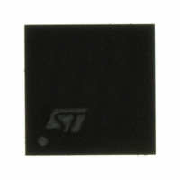
L6227Q STMicroelectronics, L6227Q Datasheet - Page 16

L6227Q
Manufacturer Part Number
L6227Q
Description
IC DRIVER FULL BRDG PWM 32VFQFPN
Manufacturer
STMicroelectronics
Type
H Bridger
Datasheet
1.L6227QTR.pdf
(27 pages)
Specifications of L6227Q
Input Type
Non-Inverting
Number Of Outputs
4
On-state Resistance
730 mOhm
Current - Output / Channel
1.4A
Current - Peak Output
2.8A
Voltage - Supply
8 V ~ 52 V
Operating Temperature
-25°C ~ 125°C
Mounting Type
Surface Mount
Package / Case
32-VFQFN, 32-VFQFPN
Product
H-Bridge Drivers
Rise Time
250 ns
Fall Time
250 ns
Supply Voltage (min)
8 V
Maximum Operating Temperature
+ 150 C
Mounting Style
SMD/SMT
Bridge Type
Full Bridge
Maximum Turn-on Delay Time
1900 ns
Minimum Operating Temperature
- 40 C
Number Of Drivers
2
For Use With
497-6817 - EVAL BOARD FOR L6227Q
Lead Free Status / RoHS Status
Lead free / RoHS Compliant
Available stocks
Company
Part Number
Manufacturer
Quantity
Price
Company:
Part Number:
L6227Q
Manufacturer:
JAE
Quantity:
24 000
Circuit description
4.6
16/27
Non-dissipative overcurrent protection
The L6227Q integrates an overcurrent detection circuit (OCD). This circuit provides
protection against a short circuit to ground or between two phases of the bridge. With this
internal over current detection, the external current sense resistor normally used and its
associated power dissipation are eliminated.
overcurrent detection circuit.
To implement the over current detection, a sensing element that delivers a small but precise
fraction of the output current is implemented with each high side power MOS. Since this
current is a small fraction of the output current there is very little additional power
dissipation. This current is compared with an internal reference current I
output current in one bridge reaches the detection threshold (typically 2.8 A) the relative
OCD comparator signals a fault condition. When a fault condition is detected, the EN pin is
pulled below the turn off threshold (1.3 V typical) by an internal open drain MOS with a pull
down capability of 4 mA. By using an external R-C on the EN pin, the off time before
recovering normal operation can be easily programmed by means of the accurate
thresholds of the logic inputs.
Figure 14. Overcurrent protection simplified schematic
Figure 15
recovering normal operation can be easily programmed by means of the accurate
thresholds of the logic inputs. It is affected whether by C
magnitude is reported in
an overcurrent has been detected depends only by C
Figure
C
the value of C
delay time and the R
The resistor R
values for R
disable time.
EN
is also used for providing immunity to pin EN against fast transient noises. Therefore
µC or LOGIC
V
DD
17.
shows the overcurrent detection operation. The disable time t
EN
R
C
EN
EN
EN
EN
and C
.
.
should be chosen as big as possible according to the maximum tolerable
should be chosen in the range from 2.2 kΩ to 180 kΩ. Recommended
EN
EN
EN
value should be chosen according to the desired disable time.
40Ω TYP.
are respectively 100 kΩ and 5.6 nF that allow obtaining 200 µs
R
Figure
DS(ON)
TO GATE
LOGIC
OPEN-DRAIN
16. The delay time t
INTERNAL
POWER SENSE
COMPARATOR
COMPARATOR
1 cell
OCD
OCD
POWER DMOS
OVER TEMPERATURE
Figure 14
n cells
OUT1
DELAY
I
1A
FROM THE
BRIDGE B
EN
/ n
(I
1A
I
A
REF
I
shows a simplified schematic of the
1A
+I
EN
value. Its magnitude is reported in
VS
2A
before turning off the bridge when
+
) / n
A
and R
I
2A
OUT2
I
2A
POWER DMOS
A
/ n
EN
n cells
values and its
HIGH SIDE DMOSs OF
DISABLE
THE BRIDGE A
REF
D01IN1337
. When the
POWER SENSE
before
1 cell
L6227Q


