IPS6011STRRPBF International Rectifier, IPS6011STRRPBF Datasheet
IPS6011STRRPBF
Specifications of IPS6011STRRPBF


Related parts for IPS6011STRRPBF

IPS6011STRRPBF Summary of contents
Page 1
INTELLIGENT POWER HIGH SIDE SWITCH Features Over temperature shutdown (with auto-restart) Short circuit protection (current limit) Reverse battery protection (turns On the MOSFET) Full diagnostic capability (short circuit to battery) Active clamp Open load ...
Page 2
Absolute Maximum Ratings Absolute maximum ratings indicate sustained limits beyond which damage to the device may occur. All voltage parameters are referenced to Ground lead. (Tambient=25°C unless otherwise specified). Symbol Parameter Vout Maximum output voltage Voffset Maximum logic ground to ...
Page 3
Static Electrical Characteristics Tj=25°C, Vcc=14V (unless otherwise specified) Symbol Parameter Rds(on) ON state resistance Tj=25°C ON state resistance Tj=150°C ON state resistance Tj=25°C, Vcc=6V ON state resistance during reverse battery Vcc op. Operating voltage range with short circuit protection V ...
Page 4
Protection Characteristics Symbol Parameter Ilim Internal current limit Tsd+ Over temperature high threshold Tsd- Over temperature low threshold Vsc Short-circuit detection voltage(2) UV+ High undervoltage lockout UV- Low undervoltage lockout VOL Off Open load detection threshold Open ...
Page 5
Functional Block Diagram All values are typical 43V Ground Disconnect GND www.irf.com 165°C Tj 158°C Vcc-gnd >UV 2.5V Shifter 2.0V Over-temp Open load off Short circuit Open load on IPS6011( VCC 37V Charge Pump Level Driver ...
Page 6
Vin Ids Vcc Vds Vds clamp See Application Notes to evaluate power dissipation Figure 1 – Active clamp waveforms 90% Vin 10% Tr-in Vcc 90% Vcc-5V Vout 10 Tr1 Tr2 Figure 3 – Switching times definitions www.irf.com T ...
Page 7
Iout, Output current (A) Figure 5 – Switching energy (µJ) Vs Output current (A) 100 10 1 0.001 0.01 Load inductance (mH) Figure 7 – Max. Output current (A) Vs Load inductance (mH) ...
Page 8
Figure 9 – Transient thermal impedance (°C/W) Vs time (s) 1.E+4 1.E+3 1.E+2 1.E+1 1.E Vcc, power supply voltage (V) Figure 11 – ...
Page 9
Case Outline - TO220 (5 lead) - Automotive Q100 PbF qualified www.irf.com IPS6011( )( )PbF ...
Page 10
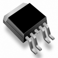
Case Outline 5 Lead - D2PAK - Automotive Q100 PbF MSL1 qualified www.irf.com IPS6011( )( )PbF ...
Page 11
Tape & Reel 5 Lead - D2PAK www.irf.com IPS6011( )( )PbF ...
Page 12
Case Outline 5 Lead – DPAK - Automotive Q100 PbF MSL1 qualified www.irf.com IPS6011( )( )PbF ...
Page 13
Tape & Reel 5 Lead – DPAK IR WORLD HEADQUARTERS: 233 Kansas St., El Segundo, California 90245 Tel: (310) 252-7105 This product has been designed and qualified for the Automotive [Q100] market. www.irf.com IPS6011( Data and specifications subject to change ...