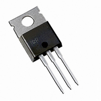
IPS021 International Rectifier, IPS021 Datasheet

IPS021
Specifications of IPS021
Available stocks
Related parts for IPS021
IPS021 Summary of contents
Page 1
... Active clamp Low current & logic level input E.S.D protection Description The IPS021/IPS021S are fully protected three terminal SMART POWER MOSFETs that feature over-current, over-temperature, ESD protection and drain to source active clamp.These devices combine a HEXFET ® POWER MOSFET and a gate driver. They offer full protection and high reliability required in harsh envi- ronments ...
Page 2
... C/W) IPS021 o (rth=80 C/W) IPS021S I sd Diode max. pulsed current pulsed P d Maximum power dissipation o (rth=62 C/W) IPS021 o (rth=80 C/W) IPS021S ESD1 Electrostatic discharge voltage ESD2 Electrostatic discharge voltage T stor. Max. storage temperature T j max. Max. junction temperature. T lead Lead temperature (soldering, 10 seconds) ...
Page 3
... Min. Typ. Max. Units Test Conditions 165 — — 4 5.5 7 1.5 2 400 — — IPS021( 5V 14V 40V 20mA (see Fig.3 & shutdown (see Fig.3 & 50mA 14V over-current triggered See figure 2 s See figure 2 nC ...
Page 4
... IPS021(S) Functional Block Diagram All values are typical IN 8 Lead Assignments 2 ( TO-220 IPS021 4 1000 Part Number DRAIN 47 V 200 k I sense T > 165°c I > Isd SOURCE 2 ( PAK (SMD220) IPS021S www.irf.com ...
Page 5
... Vcc ) Vds ( see Appl . Notes to evaluate power dissipation ) Figure 3 - Active clamp waveforms www.irf.com 90 % Vin 10 % Tr-in Tr-in t > T reset t < T reset 90 % Ids Vds Figure rise time & switching time definitions T clamp IPS021(S) Td off load Rem : V load is negative + during demagnetization Vin IN Vds Ids ...
Page 6
... IPS021(S) All curves are typical values with standard footprints. Operating in the shaded area is not recommended. 300 250 200 150 100 Figure 5 - Rds Input Voltage (V) 10 ton de lay 9 ris e tim e 8 130% rds Figure 7 - Turn-ON Delay Time, Rise Time & Time to 130% final Rds (on) (us) Vs Input Voltage (V) ...
Page 7
... Figure 9 - Turn-ON Delay Time, Rise Time & Time to 130% final Rds(on) (us Resistor ( ) Isd 25°C Ilim 25° Figure 11 - Current Iim. & I shutdown (A) Vs Vin (V) www.irf.com 10000 Figure 10 - Turn-OFF Delay Time & Fall Time (us -50 -25 Figure shutdown (A) Vs Temperature ( IPS021(S) delay off fall time Resistor ( ) 100 125 150 ...
Page 8
... Figure 15a - Iclamp (A) Vs Inductive Load (mH) IPS021 8 100 10 Load characteristic should be below this curve 1 200 Figure 14 - Ids (A) Vs Protection Resp. Time (s) IPS021 & IPS021S 10 1 Vbat = 14 V Tjini = Figure 15b - Max. Iclamp (A) Vs Inductive Load T=25°C Std. footprint T=100° ...
Page 9
... Single pulse -50 -25 Figure 17 - Input Current (uA C/W) 120% 115% 110% 105% 100% 95% 90% 85% 80% -50 -25 Figure 19 -Vin clamp and Vds clamp (%) Vs IPS021(S) Iin,on Iin,off 100 125 150 o Junction Temperature ( C) Vds clamp @ Isd Vin clamp @ 10mA 100 125 150 ...
Page 10
... IPS021(S) Case Outline NOTES: 3-Lead TO-220AB 3-Lead D 2 PAK 01-6024 00 IRGB 01-3026 01 (TO-220AB) 01-6022 00 01-0016 05 (TO-263AB) www.irf.com ...
Page 11
... Tape & Reel - D PAK (SMD220) IR WORLD HEADQUARTERS: 233 Kansas St., El Segundo, California 90245 Tel: (310) 252-7105 www.irf.com Data and specifications subject to change without notice. IPS021(S) 01-3072 00 6/11/2001 11 ...
Page 12
Note: For the most current drawings please refer to the IR website at: http://www.irf.com/package/ ...


