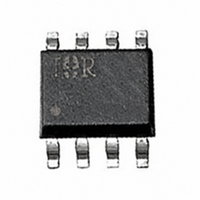
IPS521G International Rectifier, IPS521G Datasheet

IPS521G
Specifications of IPS521G
Available stocks
Related parts for IPS521G
IPS521G Summary of contents
Page 1
... Status feedback Open load detection Logic ground isolated from power ground Description The IPS521G is a fully protected five terminal high side switch with built in short circuit, over-temperature, ESD protection, inductive load capability and diagnostic feedback. The output current is controlled when it reaches I lim value. The current limitation is activated until the thermal protection acts ...
Page 2
... IPS521G Absolute Maximum Ratings Absolute maximum ratings indicate sustained limits beyond which damage to the device may occur. All voltage parameters are referenced to GROUND lead Symbol Parameter V out Maximum output voltage V offset Maximum logic ground to load ground offset Maximum Input voltage ...
Page 3
... Typ. Max. Units Test Conditions 130 — 200 0.7 — 1500 — — — 50 0.9 250 — — — IPS521G 5V, I out = 5V, I out = 2. 5V, I out = 10mA (see Fig.1 & (see Fig.1 & 2.5A 0V, V out = 1 out = 6V V out = 0V A Vdg = 5.5V 3 ...
Page 4
... IPS521G Protection Characteristics Symbol Parameter I lim Internal current limit T sd+ Over-temp. positive going threshold T sd- Over-temp. negative going threshold V Short-circuit detection voltage ( Open load detection threshold open load (3) Referenced Functional Block Diagram All values are typical 200 Lead Assignments 4 Min ...
Page 5
... Figure 3 - Switching times definition (turn-on) Turn on energy with a resistive or an inductive load www.irf.com T clamp Vin Iout limiting Ilim. T Tsd+ Tsd- (160 ° ) Figure 2 - Protection timing diagram Vin 90% Vout E1(t) 10% Iout2 Td off E2 (t) Inductive load Figure 4 - Switching times definition (turn-off) IPS521G T shutdown cycling dV/dt off Tf 5 ...
Page 6
... IPS521G Dg Vcc Out IN Gnd L Vin Vout Rem : V load is negative during demagnetization Figure 5 - Active clamp test circuit 100 Figure ds(on ( Vcc Vcc -Vsc + Iout Diag on blanking T diag Figure 6 - Diagnostic delay definitions 200% 150% 100% 50 -50 Figure 8 - Normalized R ds(on Vol Diag off blanking ...
Page 7
... Figure 9 - Rds(on out ( 1inch² footprint Rthja= 60°C Std. footprint Rthja= 100°C 100 Figure 11 - Max load current (A) Vs Tamb ( www.irf.com Figure 10 - Max. I out (A) Vs Load Inductance (uH rth SO8 std footprint 125 150 o Figure 12 - Transient Thermal Impedance ( C) IPS521G o C/W) Vs Time (s) 7 ...
Page 8
... IPS521G - Figure lim ( 10000 1000 I=Imax vs Induct.(see fig.10) 100 I=1. 0.1 Figure Load Inductance ( H) (see Fig 3500 3000 2500 2000 1500 1000 500 0 100 150 Figure on, E off ( out (A) 150 125 100 Figure 16 - Diag Blanking time ( out (A) Resistive load Eon ...
Page 9
... Figure (mA (V) Case Outline - 8 Lead SOIC www.irf.com IPS521G (MS-012AA) 01-0021 09 4/11/2000 9 ...


