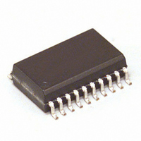
MC33287DW Freescale Semiconductor, MC33287DW Datasheet

MC33287DW
Specifications of MC33287DW
Available stocks
Related parts for MC33287DW
MC33287DW Summary of contents
Page 1
... Freescale Semiconductor, Inc. reserves the right to change the detail specifications, as may be required, to permit improvements in the design of its products. © Freescale Semiconductor, Inc., 2007. All rights reserved. AUTOMOTIVE CONTACT MONITORING AND DUAL LOW-SIDE PROTECTED DRIVER Device MC33287DW/R2 MCZ33287EG/R2 GND Sense 33287 VDD1 VDD2 ...
Page 2
... Figure 2. 33287 Simplified Internal Block Diagram 33287 2 INTERNAL BLOCK DIAGRAM IN1 IN2 IN3 IN4 IN5 Multiplexer and Diagnostic Logic DIAGD1 DIAGD2 Fault Detector Overtemperature V DD2 Current GND CD1 CD2 IN6 IN7 VDD2 OUT7 OUT1 OUTD2 Detection Control Current Limitation Analog Integrated Circuit Device Data Freescale Semiconductor ...
Page 3
... AD0 – AD2 Address 9, 11 OUTD1, Output Drain OUTD2 10 GND Ground 12, 13 CD1, CD2 Command Driver 14 OUT1 Output 1 15 OUT7 Output 7 Analog Integrated Circuit Device Data Freescale Semiconductor PIN CONNECTIONS 1 VDD1 20 VDD2 IN3 2 19 IN4 3 IN2 18 IN5 IN1 17 4 IN6 5 IN0 ...
Page 4
... T PPRT θ R J-A = 100 pF, R ZAP = 0 Ω). = 200 pF, R ZAP ZAP Value Unit 7 ±2000 ±200 -40 to 125°C °C -65 to 150 °C 0.7 W °C Note 4. 100 °C/W = 1500 Ω), ESD2 testing is performed in ZAP Analog Integrated Circuit Device Data Freescale Semiconductor ...
Page 5
... Input Current on Pin CD2 (Internal Pull Down CD2 Connected to V Leakage Current on Pin CD2 (Internal Pull-Up CD1 Connected to Ground) Notes 5 All INn and ADn inputs are connected to ground. Analog Integrated Circuit Device Data Freescale Semiconductor ≤ 4.75 V ≤ V ≤ 5.25 V, -40°C ≤ T DD1 DD2 Symbol ...
Page 6
... Analog Integrated Circuit Device Data ≤ 125°C, unless otherwise A Typ Max Unit — 4 DD1 — 3 DD1 — — V DD1 1.0 — V — 5.0 µ — 4 DD2 — — V DD2 750 — mV — 5.0 µA — 2 DD2 — — V DD2 Freescale Semiconductor ...
Page 7
... OUTPUT DRIVERS CHARACTERISTICS (OUTD1 AND OUTD2 PINS) Turn ON Delay Time Turn OFF Delay Time Output Rising Edge Output Falling Edge Difference Between Command Duration and Bit Duration Analog Integrated Circuit Device Data Freescale Semiconductor DYNAMIC ELECTRICAL CHARACTERISTICS ≤ ≤ ≤ ≤ ...
Page 8
... COMMAND BIT 80% 50% t BIT 20 FALL Figure 4. Timing Characteristics V BAT R1 = 500 Ω CD1 OUTD1 kΩ CD2 OUTD2 Figure 5. Timing Test Configuration t 80% 50% 20% t OFF t t RISE 250 pF V BAT R1 = 500 Ω 2 250 kΩ Analog Integrated Circuit Device Data Freescale Semiconductor ...
Page 9
... Notes 9 IN0 to IN6 are the normalized values. 10 DIAGD1 or DIAGD2 are the values of the selected internal fault detector. See Analog Integrated Circuit Device Data Freescale Semiconductor LOGIC COMMANDS AND REGISTERS (8) OUTD1 DIAGD1 High Level for Logic Signals High Level for Logic Signals ...
Page 10
... Unknown High Level 33287 10 Inputs AD1 AD0 Unknown Unknown Low Level High Level High Level High Level Unknown Unknown High Level Low Level High Level High Level OUT1 Unknown Unknown DIAGD1 Unknown Unknown DIAGD2 Analog Integrated Circuit Device Data Freescale Semiconductor ...
Page 11
... Vbat or GND Vbat 470nF Relay Relay (65Ω) Lamp (1,2W) Resistor Lamp V BAT 500 Ω Contact to V Analog Integrated Circuit Device Data Freescale Semiconductor TYPICAL APPLICATIONS 1 VDD1 VDD2 20 2 IN3 IN4 1 9 IN2 IN5 IN1 IN6 IN0 IN7 AD0 OUT7 AD1 ...
Page 12
... NOTE: The only difference between the low side driver 1 and 2 is the polarity of the command. Also, there is an integral pull-up at pin CD1, and an internal pull-down at pin CD2. 33287 12 IN1 IN2 IN3 IN4 IN5 LOGIC MULTIPLEXER NQ Q DIAGD1 S R VDD2 VALIM VALIM Figure 8. Electrical Schematic IN6 IN7 OUT7 OUTi DIAGD2 OUTD2 OUTD1 Analog Integrated Circuit Device Data Freescale Semiconductor ...
Page 13
... For the most current package revision, visit www.freescale.com and perform a keyword search using the “98A” listed below. Analog Integrated Circuit Device Data Freescale Semiconductor PACKAGE PACKAGE DIMENSIONS DW SUFFIX EG SUFFIX (PB-FREE) 20-PIN PLASTIC PACKAGE 98ASB42343B REV. J PACKAGE PACKAGE DIMENSIONS 33287 13 ...
Page 14
... Added note with instructions to obtain this information from Internal Block Diagram on page 2 33287 Pin Definitions on page 3 Storage Temperature on page 4 Output Resistance (Extent Limit and T Electrical Schematic on page 12 Maximum Ratings on page 4. ≤ 130°C) on page 5 J Analog Integrated Circuit Device Data Freescale Semiconductor ...
Page 15
... Freescale Semiconductor product could create a situation where personal injury or death may occur. Should Buyer ...


