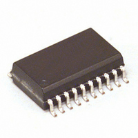
MC33289DW Freescale Semiconductor, MC33289DW Datasheet

MC33289DW
Specifications of MC33289DW
Available stocks
Related parts for MC33289DW
MC33289DW Summary of contents
Page 1
... Figure 1. 33289 Simplified Application Diagram * This document contains certain information on a new product. Specifications and information herein are subject to change without notice. © Freescale Semiconductor, Inc., 2006. All rights reserved. MOSFET DSON Device MC33289DW/R2 below 14 V BAT V PWR 5.0 V 33289 VBAT ...
Page 2
... If OLDE is a logic high, the open load circuitry is functional at the price of a higher bias current draw. OLDE pin has a pull down resistor. This is the GND pin of the device. Definition is 40 mΩ max DSON Analog Integrated Circuit Device Data Freescale Semiconductor ...
Page 3
... BAT BAT BAT OUT2 OUT2 ST2 IN2 CHANNEL 2 IN1 OLDE ST1 Analog Integrated Circuit Device Data Freescale Semiconductor V BAT Over Temp Charge Pump Input Trigger U.V.& O.V. Lockout Open Load GND Figure 3. Simplified Internal Block Diagram PIN CONNECTIONS BAT BAT ...
Page 4
... ELECTRICAL CHARACTERISTICS MAXIMUM RATINGS Symbol Value Unit V -0 BAT V -4 OUT OUT V -0 -0 +/-4 +/-2000 V ESD1 V +/-200 V ESD2 °C T -40 to 150 J °C T -55 to 150 ST °C THJA °C THJL1 °C THJL2 °C THJL3 Analog Integrated Circuit Device Data Freescale Semiconductor ...
Page 5
... Input Capacitance IN1, IN2 kΩ @ 100 kHz IN STATUS CHARACTERISTICS Status Voltage mA; Output in fault ST Status Leakage Current Analog Integrated Circuit Device Data Freescale Semiconductor 7.0 V ≤ V ≤ 40°C ≤ T ≤ 125°C, GND = 0 V SUP 25°C under nominal conditions unless otherwise noted. A Symbol V BAT I ...
Page 6
... INOL unless otherwise noted. Typical Min Typ Max 80 4.0 9.0 150 165 175 0.1 2.0 4.75 6.0 0.3 0.6 1.0 200 290 400 1.5 2.4 3.5 1.5 2.5 3.5 Analog Integrated Circuit Device Data Freescale Semiconductor Unit pF A °C ° µ ...
Page 7
... OLSTDT T OLDBT 3.0 S RPOUT1 1.0 S RPOUT2 0.1 S RNOUT 1.0 t DON 1.0 t DOFF 1.0 unless otherwise noted. Typical Typ Max Unit µs 30 µs 50 µs 100 µ V/µs 20 V/µs 3.0 V/µs 20 µs 2.5 15 µs 5.0 15 Analog Integrated Circuit Device Data Freescale Semiconductor ...
Page 8
... CHANNEL 2 Input Trigger U.V.& O.V. Lockout GND Figure 4. MC33289 Typical Application IN1 IN2 OUT1 VBAT VBAT VBAT VBAT Thermal Sensor Over Temp OUT1 OUT1 Over LOAD Current Open Load CHANNEL 1 OUT2 ST1 ST2 Analog Integrated Circuit Device Data Freescale Semiconductor ...
Page 9
... For the most current package revision, visit Analog Integrated Circuit Device Data Freescale Semiconductor PACKAGING PACKAGE DIMENSIONS www.freescale.com and perform a keyword search using the “98A” listed below DW SUFFIX 20-PIN PLASTIC PACKAGE 98ASB42343B ISSUE J PACKAGING PACKAGE DIMENSIONS 33289 9 ...
Page 10
... REVISION HISTORY REVISION DATE DESCRIPTION OF CHANGES • Implemented Revision History page 6/2006 4.0 • Converted to Freescale format • Updated to the prevailing form and style 33289 10 REVISION HISTORY Analog Integrated Circuit Device Data Freescale Semiconductor ...
Page 11
... Freescale Semiconductor product could create a situation where personal injury or death may occur. Should Buyer ...


