MC33880DWB Freescale Semiconductor, MC33880DWB Datasheet
MC33880DWB
Specifications of MC33880DWB
Available stocks


Related parts for MC33880DWB


MC33880DWB Summary of contents
Page 1
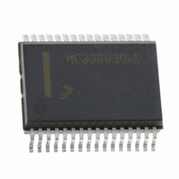
... This document contains certain information on a new product. Specifications and information herein are subject to change without notice. © Freescale Semiconductor, Inc., 2009. All rights reserved. DW SUFFIX EG SUFFIX (PB-FREE) 98ASB42345B 28-PIN SOICW < 24.5 V MC33880DW/R2 PWR MCZ33880EG/ 95°C PWR MC33880DWB/R2 MCZ33880EW/R2 V PWR V S 33880 VPWR D1 5 VDD D4 D5 ...
Page 2
... Open/Short Comparator VPWR Overvoltage Shutdown/POR Sleep State GND Open Outputs Load D7 Detect Current D8 ~650 μ Source S4 ~1.5 V Open/Short Threshold Outputs Outputs D6 Open Load Detect Current ~650 μA S5 Source Outputs ~1.5 V Open/Short Threshold Analog Integrated Circuit Device Data Freescale Semiconductor Drain Drain ...
Page 3
... Output 7 MOSFET source pins. 27 VPWR Power supply pin to the 33880. VPWR has internal reverse battery protection SPI control data output pin from the 33880 to the MCU fault specific output has fault. Analog Integrated Circuit Device Data Freescale Semiconductor PIN CONNECTIONS GND 1 28 VDD 2 27 ...
Page 4
... SPI control data output pin from the 33880 to the MCU fault specific output has fault. 33880 4 GND 1 32 VDD TGND 8 25 TGND IN6 SCLK 16 17 Figure 4. 32-Pin Connections Definition DO VPWR TGND TGND IN5 CS DI below 3.9 V). DD Analog Integrated Circuit Device Data Freescale Semiconductor ...
Page 5
... Freescale’s Package Reflow capability meets Pb-free requirements for JEDEC standard J-STD-020C. For Peak Package Reflow Temperature and Moisture Sensitivity Levels (MSL www.freescale.com, search by part number [e.g. remove prefixes/suffixes and enter the core ID to view all orderable parts (i.e. MC33xxxD enter 33xxx), and review parametrics. Analog Integrated Circuit Device Data Freescale Semiconductor ELECTRICAL CHARACTERISTICS MAXIMUM RATINGS (8) ...
Page 6
... PWR Typ Max Unit V – 24.5 8 μA 2.0 5.0 5 0.8 2.5 V – 5.25 V 2.6 4.0 mA 4.3 4.7 V 150 300 mV Ω 0.75 1.1 0.55 0.85 0.45 0.80 A 1.4 2.0 V – 3.0 mA 0.55 1 -20 -25 μA 1.0 7.0 ° – 185 C ° Freescale Semiconductor ...
Page 7
... Input Capacitance on SCLK, DI, Tri-State DO, IN5, IN6, EN Notes 12. Upper and lower logic threshold voltage levels apply to DI, 13. This parameter is guaranteed by design but is not production tested. Analog Integrated Circuit Device Data Freescale Semiconductor STATIC ELECTRICAL CHARACTERISTICS ≤ 5.25 V, 9.0 V ≤ V ≤ -40°C ≤ PWR Symbol ...
Page 8
... Analog Integrated Circuit Device Data Freescale Semiconductor Unit V/μs V/μs V/μs V/μs μs μs μs MHz μ ...
Page 9
... Under CS Test NOTE: C represents the total capacitance of the test L fixture and probe. Figure 7. Enable and Disable Time Test Circuit Analog Integrated Circuit Device Data Freescale Semiconductor TIMING DIAGRAMS t t DI(SU) DI(HOLD) MSB in t VALID MSB out Figure 5. SPI Timing Diagram ...
Page 10
... High) Figure 11. Turn-ON/OFF Waveforms t t R(DI) F(DI) < < 5.0 V 90 DO(EN) DO(DIS) V Tri-State 90% 10% t SO(DIS DO(EN) DO(DIS) V 90% V Tri-State 10 R(DI) F(DI) < < 90 DO(EN) DO(DIS) V Tri-State 90% 10% t SO(DIS DO(EN) DO(DIS) 90% V Tri-State 10% Analog Integrated Circuit Device Data Freescale Semiconductor ...
Page 11
... V PWR Figure 14. Sleep State I PWR 1 PWR 1.2 1.0 0.8 0.6 0.4 0 (V) PWR Figure 16. R vs. V DS(ON) PWR Analog Integrated Circuit Device Data Freescale Semiconductor -40 -25 -40 -25 75 100 125 ° C) Figure 13. Sleep State I 1.4 V 1.2 1.0 0.8 0.6 0.4 0.2 ...
Page 12
... Figure 20. Sleep State Output Leakage vs. V 33880 12 1.4 1.2 1.0 0.8 0.6 0.4 0 100 125 ° C) Figure 19. Open Load Detect Current vs 25°C A 1.2 1.0 0.8 0.6 0.4 0 (V) PWR T = 25° (V) PWR PWR 20 25 PWR Analog Integrated Circuit Device Data Freescale Semiconductor 25 ...
Page 13
... DI pin will program the output off. The specific output will turn off with the rising edge of the program the eight outputs of the 33880 device on or off, enter Analog Integrated Circuit Device Data Freescale Semiconductor FUNCTIONAL DESCRIPTION INTRODUCTION The 33880 device uses high-efficiency updrain power ...
Page 14
... High-Side Drive configurations, the source pins are connected directly to the load. In Low-Side Drive configurations the source is connected to ground. All outputs may be configured individually as desired. When High-Side drive is used, the 33880 will limit the negative transient for inductive loads to -20 V. Analog Integrated Circuit Device Data Freescale Semiconductor ...
Page 15
... MCU. During each clock cycle output status from the daisy chain, the 33880 is being transferred to the MCU via the Analog Integrated Circuit Device Data Freescale Semiconductor OPERATIONAL MODES Master In Slave Out (MISO) line. On rising edge of stored in the input register is then transferred to the output driver ...
Page 16
... FUNCTIONAL DEVICE OPERATION OPERATIONAL MODES 33880 16 Analog Integrated Circuit Device Data Freescale Semiconductor ...
Page 17
... Bus integrity is confirmed by the MCU receiving the same bit pattern it Analog Integrated Circuit Device Data Freescale Semiconductor sent. Please note that the second byte the MCU sends to the device is the command byte and will be transferred to the outputs with rising edge of ≤ ...
Page 18
... If load reverse battery protection is desired, a diode must be placed in series with the load Drain Voltage CL Clamp Energy ( Current Area ( Time GND V BAT ) GND Time Current Area ( Clamp Energy ( Source Voltage Analog Integrated Circuit Device Data Freescale Semiconductor ) ) ...
Page 19
... All outputs assuming the previous state upon recovery from overvoltage. Overtemperature Only the output experiencing an overtemperature fault shuts down. Output assumes previous state upon recovery from overtemperature. Analog Integrated Circuit Device Data Freescale Semiconductor LOGIC COMMANDS AND REGISTERS LSB OUT3 OUT2 OUT1 = ...
Page 20
... PACKAGING PACKAGE DIMENSIONS For the most current package revision, visit www.freescale.com and perform a keyword search using “98ASB42345B”. 33880 20 PACKAGING PACKAGE DIMENSIONS DW SUFFIX EG SUFFIX (PB-FREE) 28-PIN PLASTIC PACKAGE 98ASB42345B REV G Analog Integrated Circuit Device Data Freescale Semiconductor ...
Page 21
... Analog Integrated Circuit Device Data Freescale Semiconductor PACKAGE DIMENSIONS (CONTINUED) DW SUFFIX EG SUFFIX (PB-FREE) 28-PIN PLASTIC PACKAGE 98ASB42345B REV G PACKAGING PACKAGE DIMENSIONS 33880 21 ...
Page 22
... PACKAGING PACKAGE DIMENSIONS 33880 22 PACKAGE DIMENSIONS (CONTINUED) DWB SUFFIX EW SUFFIX (PB-FREE) 32-PIN PLASTIC PACKAGE 98ASB42345B REV B Analog Integrated Circuit Device Data Freescale Semiconductor ...
Page 23
... Analog Integrated Circuit Device Data Freescale Semiconductor PACKAGE DIMENSIONS (CONTINUED) DWB SUFFIX EW SUFFIX (PB-FREE) 32-PIN PLASTIC PACKAGE 98ASB42345B REV B PACKAGING PACKAGE DIMENSIONS 33880 23 ...
Page 24
... Changed 32 pin SOICW, pins 8, 9, 24, 25 from GND to TGND on page 4. 6 1/2009 • Corrected Notes for Peak Package Reflow in Maximum Rating Table. 7.0 33880 24 REVISION HISTORY Peak Package Reflow Temperature During Reflow (8) (9) , Analog Integrated Circuit Device Data Freescale Semiconductor ...
Page 25
... Freescale Semiconductor product could create a situation where personal injury or death may occur. Should Buyer ...