E-L6258E STMicroelectronics, E-L6258E Datasheet
E-L6258E
Specifications of E-L6258E
Available stocks


Related parts for E-L6258E


E-L6258E Summary of contents
Page 1
... DC motors. Table 1. Device summary Order code L6258E (Replaced by E-L6258EX and E- L6258EXTR) March 2010 This is information on a product still in production but not recommended for new designs. high current DMOS universal motor driver The power stage is a dual DMOS full bridge capable of sustaining up to 40V, and includes the diodes for current recirculation ...
Page 2
... Phase input ( 2.4 Triangular generator . . . . . . . . . . . . . . . . . . . . . . . . . . . . . . . . . . . . . . . . . 13 2.5 Charge pump circuit . . . . . . . . . . . . . . . . . . . . . . . . . . . . . . . . . . . . . . . . . 13 2.6 Current control loop . . . . . . . . . . . . . . . . . . . . . . . . . . . . . . . . . . . . . . . . . 14 2.7 Current control loop compensation . . . . . . . . . . . . . . . . . . . . . . . . . . . . . 15 3 PWM current control loop . . . . . . . . . . . . . . . . . . . . . . . . . . . . . . . . . . . 16 3.1 Open loop transfer function analysis . . . . . . . . . . . . . . . . . . . . . . . . . . . . 16 3.2 Power amplifier . . . . . . . . . . . . . . . . . . . . . . . . . . . . . . . . . . . . . . . . . . . . . 17 3.3 Load attenuation . . . . . . . . . . . . . . . . . . . . . . . . . . . . . . . . . . . . . . . . . . . . 18 3.4 Error amplifier and sense amplifier . . . . . . . . . . . . . . . . . . . . . . . . . . . . . . 19 3.5 Effect of the Bemf on the current control loop stability ...
Page 3
... L6258E List of tables Table 1. Device summary . . . . . . . . . . . . . . . . . . . . . . . . . . . . . . . . . . . . . . . . . . . . . . . . . . . . . . . . . . 1 Table 2. Absolute maximum rating . . . . . . . . . . . . . . . . . . . . . . . . . . . . . . . . . . . . . . . . . . . . . . . . . . . 5 Table 3. Pin functions . . . . . . . . . . . . . . . . . . . . . . . . . . . . . . . . . . . . . . . . . . . . . . . . . . . . . . . . . . . . . 6 Table 4. Electrical characteristics . . . . . . . . . . . . . . . . . . . . . . . . . . . . . . . . . . . . . . . . . . . . . . . . . . . . 8 Table 5. Current levels . . . . . . . . . . . . . . . . . . . . . . . . . . . . . . . . . . . . . . . . . . . . . . . . . . . . . . . . . . . 12 Table 6. Charge pump capacitor's values Table 7. Document revision history . . . . . . . . . . . . . . . . . . . . . . . . . . . . . . . . . . . . . . . . . . . . . . . . . 30 Doc ID 8688 Rev 9 List of tables 3/31 ...
Page 4
... Figure 9. Aloop bode plot (compensated Figure 10. Electrical model of the load Figure 11. Typical application circuit . . . . . . . . . . . . . . . . . . . . . . . . . . . . . . . . . . . . . . . . . . . . . . . . . . 25 Figure 12. Half step operation mode timing diagram . . . . . . . . . . . . . . . . . . . . . . . . . . . . . . . . . . . . . . 27 Figure 13. 4 bit microstep operation mode timing diagram . . . . . . . . . . . . . . . . . . . . . . . . . . . . . . . . . 28 Figure 14. PowerSO36 mechanical data & package dimensions . . . . . . . . . . . . . . . . . . . . . . . . . . . . 29 4/31 Doc ID 8688 Rev 9 L6258E ...
Page 5
... Description Supply voltage Logic supply voltage Reference voltage Output current (peak) Output current (continuous) Logic input voltage range Bootstrap supply Maximum Vgate applicable Junction temperature Storage temperature range Doc ID 8688 Rev 9 Block diagram C BOOT VS EA_OUT1 VBOOT TRI_0 + C - POWER BRIDGE 1 + TRI_180 C - TRI_0 ...
Page 6
... These TTL compatible logic inputs set the direction of PH_1, PH_2 current flow through the load. A high level causes current to flow from OUTPUT A to OUTPUT B. Logic input of the internal DAC (1). The output voltage of the I DAC is a percentage of the Vref voltage applied according to 1_1 ...
Page 7
... Note: The number in parenthesis shows the relevant Power Bridge of the circuit. Pins 18, 19, 1 and 36 are connected together. Name V (5V) Supply voltage input for logic circuitry DD GND Power ground connection of the internal charge pump circuit V Charge pump oscillator output CP1 V Input for external charge pump capacitor ...
Page 8
... Block diagram Figure 3. Thermal characteristics Conditions pad layout + ground layers + 16 via hol PCB ref.: 4 LAYER pad layout + ground layers PCB ref.: 4 LAYER pad layout + 6cm2 on board heat sink PCB ref.: 2 LAYER Table 4. Electrical characteristics (V S Parameter V Supply voltage S V Logic supply voltage ...
Page 9
... ERROR AMPLIFIER G Open loop voltage gain V SR Output slew rate GBW Gain bandwidth product 1. Chopping frequency is twice fosc value. 2. This is true for all the logic inputs except the disable input. = 40V 5V 25°; unless otherwise specified Description Test condition C (1) ...
Page 10
... Now just increasing the duty cycle of the IN_A signal and decreasing the duty cycle of IN_B signal we drive positive current into the load. In this way the two outputs are not in phase, and the current can flow into the load trough the diagonal bridge formed by T1 and T4 when the output OUT_A is driven to V ...
Page 11
... L6258E 2.1 Reference voltage The voltage applied to VREF pin is the reference for the internal DAC and, together with the sense resistor value, defines the maximum current into the motor winding according to the following relation: where R = sense resistor value s Figure 4. Power bridge configuration ...
Page 12
... Functional description Figure 5. Current control loop block diagram INPUT TRANSCONDUCTANCE AMPL. ia VREF VDAC DAC - Gin=1/Ra 2.2 Input logic (I The current level in the motor winding is selected according to this table: Table 5. Current levels 12/31 Tri_0 ERROR AMPL Tri_180 VSENSE + Gs=1/Rb SENSE TRANSCONDUCTANCE AMPL. ...
Page 13
... Charge pump circuit To ensure the correct driving of the high side drivers a voltage higher than Vs is supplied on the Vboot pin. This boostrap voltage is not needed for the low side power DMOS transistors because their sources terminals are grounded. To produce this voltage a charge pump method is used made by using two external capacitors ...
Page 14
... OUTB) are generated by the use of the two comparators having as reference two triangular wave signals Tri_0 and Tri_180 of the same amplitude, the same average value (in our case Vr), but with a 180° of phase shift each other. The two triangular wave references are respectively applied to the inverting input of the first comparator and to the non inverting input of the second comparator ...
Page 15
... OUT_A through the motor winding to OUT_B. With a negative differential voltage V unbalanced respected Vr. In this case the output of the first comparator is a square wave with a duty cycle lower than 50%, while the output of the second comparator is a square wave with a duty cycle higher than 50%. ...
Page 16
... It is clear that to have a good performance of the current control loop, the error amplifier must have an high DC gain and a large bandwidth. 16/31 Figure 5 ...
Page 17
... RC network connected between the output and the negative input of the same. For the evaluation of the stability of the system, we have to consider the open loop gain of the current control loop: where AC... is the gain of the blocks that refers to the error, power and sense amplifier plus the attenuation of the load block ...
Page 18
... We will considered the effect of the Bemf voltage of the motor in the next chapter. The input of this block is the PWM voltage of the power amplifier and as output we have the voltage across the sense resistor produced by the current flowing into the motor winding. ...
Page 19
... Figure 7. Ax bode plot The Bode plot of the Ax|dB function shows a DC gain of -1.9dB and a pole at 163Hz clear now that (because of the negative gain of the Ax function), Bx function must have an high DC gain in order to increment the total open loop gain increasing the bandwidth too. ...
Page 20
... Aloop given by the following equation: The total Aloop has an high DC gain of 78.1dB with a bandwidth of 15KHz, but the problem in this case is the stability of the system; in fact the total Aloop cross the zero dB axis with a slope of -40dB/decade. Now it is necessary to compensate the error amplifier in order to obtain a total Aloop with an high DC gain and a large bandwidth ...
Page 21
... L6258E In this case the Bx block has a DC gain equal to the open loop and equal to zero at a frequency given by the following formula: In order to cancel the pole of the load, the zero of the Bx block must be located at the same frequency of 163Hz; so now we have to find a compromise between the resistor and the capacitor of the compensation network ...
Page 22
... Figure 9. Aloop bode plot (compensated) We can see that the effect of the load pole is cancelled by the zero of the Bx block ; the total Aloop cross a the 0dB axis with a slope of -20dB/decade, having in this way a stable system with an high gain at low frequency and a bandwidth of around 8KHz. ...
Page 23
... Bemf of the motor is not critical because the phase margin remains the same. Practically the only effect of the Bemf is to limit the gain of the total Aloop with a consequent variation of the bandwidth of the system. ...
Page 24
... The EA_IN1 and EA_IN2 pins carry out high impedance lines and care must be taken to avoid coupled noise on this signals. The suggestion is to put the components connected to this pins close to the L6258E, to surround them with ground tracks and to keep as far as possible fast switching outputs of the device. Remember also an 1 Mohm resistor between EA_INx and EA_OUTx to avoid output current spike during supply startup/shutdown ...
Page 25
... Motor selection Some stepper motor have such high core losses that they are not suitable for switch mode current regulation. Furthermore, some stepper motors are not designed for continuous operating at maximum current. Since the circuit can drive a constant current through the motor, its temperature might exceed, both at low and high speed operation ...
Page 26
... It's important to separate on the PCB board the logic and power grounds and the internal charge pump circuit ground avoiding that ground traces of the logic signals cross the ground traces of the power signals. Because the IC uses the board as a heat sink, the dissipating copper area must be sized in accordance with the required value of R 26/31 ...
Page 27
... L6258E 5 Operation mode time diagrams Figure 12. Half step operation mode timing diagram (Phase - DAC input and motor current) Phase 1 Phase 2 I0_1 DAC 1 I1_1 Inputs I2_1 I3_1 I0_2 I1_2 DAC 2 Inputs I2_2 I3_2 100% 71.4% Motor drive Current 1 -71.4% -100% 100% 71.4% ...
Page 28
... Operation mode time diagrams Figure 13. 4 bit microstep operation mode timing diagram (Phase - DAC input and motor current) Position Phase Phase 5V 2 I0_1 0 5V I1_1 0 DAC 1 Inputs 5V I2_1 0 5V I3_1 0 5V I0_2 0 DAC 2 Inputs 5V I1_2 0 5V I2_2 0 I3_2 0 Motor drive Current 1 ...
Page 29
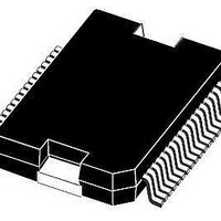
... L6258E 6 Package information In order to meet environmental requirements, ST offers these devices in different grades of ECOPACK® packages, depending on their level of environmental compliance. ECOPACK® specifications, grade definitions and product status are available at: www.st.com. ECOPACK® trademark. Figure 14. PowerSO36 mechanical data & package dimensions DIM ...
Page 30
... Revision 5 First Issue in EDOCS DMS Restyling of the graphic form, changed all V delete TSD parameter in the Electrical characteristic on 6 NOT FOR NEW DESIGN, it has been replaced by equivalent L6258EX. Changed on the page 5 the f 7 18.5kHz Document reformatted. 8 Modified the ACpw formula in ...
Page 31
... The ST logo is a registered trademark of STMicroelectronics. All other names are the property of their respective owners. Australia - Belgium - Brazil - Canada - China - Czech Republic - Finland - France - Germany - Hong Kong - India - Israel - Italy - Japan - Malaysia - Malta - Morocco - Philippines - Singapore - Spain - Sweden - Switzerland - United Kingdom - United States of America Please Read Carefully: © ...