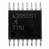
A3950SLP-T Allegro Microsystems Inc, A3950SLP-T Datasheet

A3950SLP-T
Specifications of A3950SLP-T
Related parts for A3950SLP-T
A3950SLP-T Summary of contents
Page 1
Features and Benefits ▪ Low R outputs DS(on) ▪ Overcurrent protection ▪ Motor lead short-to-supply protection ▪ Short-to-ground protection ▪ Sleep function ▪ Synchronous rectification ▪ Diagnostic output ▪ Internal undervoltage lockout (UVLO) ▪ Crossover-current protection Packages: Package LP, 16 ...
Page 2
... A3950 Selection Guide Part Number A3950SLP-T 96 pieces / tube A3950SLPTR-T 13 in. reel, 4000 pieces / reel A3950SEU-T 92 pieces / tube A3950SEUTR-T 7 in. reel, 1500 pieces / reel Absolute Maximum Ratings Characteristic Load Supply Voltage Output Current Sense Voltage VBB to OUTx OUTx to SENSE Logic Input Voltage ...
Page 3
A3950 VREG 0.22 μ MODE PHASE V DD ENABLE 5 kΩ SLEEP 5 kΩ NFAULT Terminal List Table Name EU NFAULT 15 MODE 16 PHASE 1 GND 2, 12 SLEEP 3 ENABLE 4 OUTA 6 SENSE 7 VBB ...
Page 4
A3950 ELECTRICAL CHARACTERISTICS 25°C, V Characteristics Motor Supply Current PHASE, ENABLE, MODE Input Voltage SLEEP Input Voltage PHASE, MODE Input Current 1 ENABLE Input Current SLEEP Input Current NFAULT Output Voltage Input Hysteresis, except SLEEP Output ...
Page 5
A3950 SLEEP ENABLE PHASE MODE OUTA OUTB 0 I OUTX OutA 3 A Charge pump and VREG power-on delay (≈200 μs) DMOS Full-Bridge Motor Driver Timing Diagram: PWM Control ...
Page 6
A3950 V OUTA High-Z V OUTB I PEAK I OCP I OUTx ENABLE, Source or Sink BLANK Charge Pump Counter NFAULT Motor lead short condition DMOS Full-Bridge Motor Driver Timing Diagram: Overcurrent Control t t BLANK OCP Normal dc motor ...
Page 7
A3950 Device Operation. The A3950 is designed to operate one DC motor. The output drivers are all low R drivers that feature internal synchronous rectification to reduce power dissipation. PHASE and ENABLE inputs allow two-wire control with an additional MODE ...
Page 8
A3950 NFAULT low, but does not disable the operation of the chip. If the die temperature increases further, to approximately 175°C, the full-bridge outputs will be disabled until the internal temperature falls below a hysteresis of 15°C. Overcurrent Protection. Referring ...
Page 9
A3950 Power Dissipation. First order approximation of power dissipation in the A3950 can be calculated by first examining the power dissipation in the full-bridge during each of the operation modes. The A3950 features synchronous rectifica- tion, a feature that effectively ...
Page 10
A3950 SENSE Pin. A low value resistor can be placed between the SENSE pin and ground for current sensing purposes. To mini- mize ground-trace IR drops in sensing the output current level, the current sensing resistor should have an independent ...
Page 11
A3950 All dimensions reference only, not for tooling use. (reference JEDEC MO-220WGGC-4) Dimensions in millimeters U.S. Customary dimensions (in.) in brackets, for reference only Dimensions exclusive of mold flash, gate burrs, and dambar protrusions Exact case and lead configuration at ...
Page 12
A3950 LP Package, 16 Pin TSSOP with Exposed Thermal Pad 16X 0.10 [.004] C 0.30 .012 16X 0.19 .007 0.10 [.004 0.45 .018 NOM 1.65 .065 NOM 2X0.20 .008 MIN The products described here are manufactured ...


