MC33035PG ON Semiconductor, MC33035PG Datasheet - Page 9
MC33035PG
Manufacturer Part Number
MC33035PG
Description
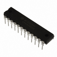
IC CTRLR MOTOR DC BRUSHLSS 24DIP
Manufacturer
ON Semiconductor
Type
Brushless DC Motor Controllerr
Datasheet
1.NCV33035DWR2G.pdf
(28 pages)
Specifications of MC33035PG
Applications
DC Motor Controller, Brushless (BLDC)
Number Of Outputs
1
Current - Output
100mA
Voltage - Load
5.9 V ~ 6.5 V
Voltage - Supply
10 V ~ 30 V
Operating Temperature
-40°C ~ 85°C
Mounting Type
Through Hole
Package / Case
24-DIP (0.300", 7.62mm)
Operating Current
20mA
Operating Temperature Classification
Industrial
Package Type
PDIP
Operating Supply Voltage (min)
10V
Operating Supply Voltage (max)
30V
Operating Supply Voltage
10 V to 30 V
Supply Current
20 mA
Mounting Style
Through Hole
Lead Free Status / RoHS Status
Lead free / RoHS Compliant
Other names
MC33035PGOS
Available stocks
Company
Part Number
Manufacturer
Quantity
Price

Part Number:
MC33035PG
Manufacturer:
MOTOROLA/摩托罗拉
Quantity:
20 000


INTRODUCTION
monolithic DC brushless motor controllers produced by
Motorola. It contains all of the functions required to
implement a full−featured, open loop, three or four phase
motor control system. In addition, the controller can be made
to operate DC brush motors. Constructed with Bipolar
Analog technology, it offers a high degree of performance and
ruggedness in hostile industrial environments. The MC33035
contains a rotor position decoder for proper commutation
sequencing, a temperature compensated reference capable of
supplying a sensor power, a frequency programmable
sawtooth oscillator, a fully accessible error amplifier, a pulse
width modulator comparator, three open collector top drive
outputs, and three high current totem pole bottom driver
outputs ideally suited for driving power MOSFETs.
consisting of undervoltage lockout, cycle−by−cycle current
limiting with a selectable time delayed latched shutdown
mode, internal thermal shutdown, and a unique fault output
that can easily be interfaced to a microprocessor controller.
control, forward or reverse rotation, run enable, and
dynamic braking. In addition, the MC33035 has a 60°/120°
select pin which configures the rotor position decoder for
either 60° or 120° sensor electrical phasing inputs.
FUNCTIONAL DESCRIPTION
Figure 19 with various applications shown in Figures 36, 38,
39, 43, 45, and 46. A discussion of the features and function
of each of the internal blocks given below is referenced to
Figures 19 and 36.
Rotor Position Decoder
sensor inputs (Pins 4, 5, 6) to provide the proper sequencing
of the top and bottom drive outputs. The sensor inputs are
designed to interface directly with open collector type Hall
Effect switches or opto slotted couplers. Internal pull−up
resistors are included to minimize the required number of
external components. The inputs are TTL compatible, with
their thresholds typically at 2.2 V. The MC33035 series is
designed to control three phase motors and operate with four
of the most common conventions of sensor phasing. A
60°/120° Select (Pin 22) is conveniently provided and
affords the MC33035 to configure itself to control motors
having either 60°, 120°, 240° or 300° electrical sensor
phasing. With three sensor inputs there are eight possible
input code combinations, six of which are valid rotor
positions. The remaining two codes are invalid and are
usually caused by an open or shorted sensor line. With six
valid input codes, the decoder can resolve the motor rotor
position to within a window of 60 electrical degrees.
direction of motor rotation by reversing the voltage across
The MC33035 is one of a series of high performance
Included in the MC33035 are protective features
Typical motor control functions include open loop speed
A representative internal block diagram is shown in
An internal rotor position decoder monitors the three
The Forward/Reverse input (Pin 3) is used to change the
MC33035, NCV33035
http://onsemi.com
9
the stator winding. When the input changes state, from high
to low with a given sensor input code (for example 100), the
enabled top and bottom drive outputs with the same alpha
designation are exchanged (A
In effect, the commutation sequence is reversed and the
motor changes directional rotation.
Enable (Pin 7). When left disconnected, an internal 25 μA
current source enables sequencing of the top and bottom
drive outputs. When grounded, the top drive outputs turn off
and the bottom drives are forced low, causing the motor to
coast and the Fault output to activate.
safety to be designed into the final product. Braking is
accomplished by placing the Brake Input (Pin 23) in a high
state. This causes the top drive outputs to turn off and the
bottom drives to turn on, shorting the motor−generated back
EMF. The brake input has unconditional priority over all
other inputs. The internal 40 kΩ pull−up resistor simplifies
interfacing with the system safety−switch by insuring brake
activation if opened or disconnected. The commutation
logic truth table is shown in Figure 20. A four input NOR
gate is used to monitor the brake input and the inputs to the
three top drive output transistors. Its purpose is to disable
braking until the top drive outputs attain a high state. This
helps to prevent simultaneous conduction of the the top and
bottom power switches. In half wave motor drive
applications, the top drive outputs are not required and are
normally left disconnected. Under these conditions braking
will still be accomplished since the NOR gate senses the
base voltage to the top drive output transistors.
Error Amplifier
with access to both inputs and output (Pins 11, 12, 13) is
provided to facilitate the implementation of closed loop
motor speed control. The amplifier features a typical DC
voltage gain of 80 dB, 0.6 MHz gain bandwidth, and a wide
input common mode voltage range that extends from ground
to V
amplifier is configured as a unity gain voltage follower with
the noninverting input connected to the speed set voltage
source. Additional configurations are shown in Figures 31
through 35.
Oscillator
programmed by the values selected for timing components
R
Output (Pin 8) through resistor R
internal discharge transistor. The ramp peak and valley
voltages are typically 4.1 V and 1.5 V respectively. To
provide a good compromise between audible noise and
output switching efficiency, an oscillator frequency in the
range of 20 to 30 kHz is recommended. Refer to Figure 1 for
component selection.
T
Motor on/off control is accomplished by the Output
Dynamic motor braking allows an additional margin of
A high performance, fully compensated error amplifier
The frequency of the internal ramp oscillator is
and C
ref
. In most open loop speed control applications, the
T
. Capacitor C
T
is charged from the Reference
T
to A
T
B
and discharged by an
, B
T
to B
B
, C
T
to C
B
).
Related parts for MC33035PG
Image
Part Number
Description
Manufacturer
Datasheet
Request
R

Part Number:
Description:
ON Semiconductor [VOLTAGE REGULATOR]
Manufacturer:
ON Semiconductor
Datasheet:
Part Number:
Description:
357-036-542-201 CARDEDGE 36POS DL .156 BLK LOPRO
Manufacturer:
ON Semiconductor
Datasheet:
Part Number:
Description:
357-036-542-201 CARDEDGE 36POS DL .156 BLK LOPRO
Manufacturer:
ON Semiconductor
Datasheet:
Part Number:
Description:
357-036-542-201 CARDEDGE 36POS DL .156 BLK LOPRO
Manufacturer:
ON Semiconductor
Datasheet:
Part Number:
Description:
357-036-542-201 CARDEDGE 36POS DL .156 BLK LOPRO
Manufacturer:
ON Semiconductor
Datasheet:
Part Number:
Description:
357-036-542-201 CARDEDGE 36POS DL .156 BLK LOPRO
Manufacturer:
ON Semiconductor
Datasheet:
Part Number:
Description:
357-036-542-201 CARDEDGE 36POS DL .156 BLK LOPRO
Manufacturer:
ON Semiconductor
Datasheet:
Part Number:
Description:
357-036-542-201 CARDEDGE 36POS DL .156 BLK LOPRO
Manufacturer:
ON Semiconductor
Datasheet:
Part Number:
Description:
357-036-542-201 CARDEDGE 36POS DL .156 BLK LOPRO
Manufacturer:
ON Semiconductor
Datasheet:
Part Number:
Description:
357-036-542-201 CARDEDGE 36POS DL .156 BLK LOPRO
Manufacturer:
ON Semiconductor
Datasheet:
Part Number:
Description:
357-036-542-201 CARDEDGE 36POS DL .156 BLK LOPRO
Manufacturer:
ON Semiconductor
Datasheet:
Part Number:
Description:
Manufacturer:
ON Semiconductor
Datasheet:
Part Number:
Description:
Manufacturer:
ON Semiconductor
Datasheet:
Part Number:
Description:
Manufacturer:
ON Semiconductor
Datasheet: