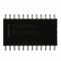
MC33035DWR2G ON Semiconductor, MC33035DWR2G Datasheet - Page 12

MC33035DWR2G
Manufacturer Part Number
MC33035DWR2G
Description
IC CTRLR MOTOR DC BRSHLSS 24SOIC
Manufacturer
ON Semiconductor
Type
Brushless DC Motor Controllerr
Datasheet
1.NCV33035DWR2G.pdf
(28 pages)
Specifications of MC33035DWR2G
Applications
DC Motor Controller, Brushless (BLDC)
Number Of Outputs
1
Current - Output
100mA
Voltage - Load
5.9 V ~ 6.5 V
Voltage - Supply
10 V ~ 30 V
Operating Temperature
-40°C ~ 85°C
Mounting Type
Surface Mount
Package / Case
24-SOIC (7.5mm Width)
Operating Supply Voltage
10 V to 30 V
Supply Current
20 mA
Mounting Style
SMD/SMT
Operating Current
20mA
Operating Temperature Classification
Industrial
Package Type
SOIC
Operating Supply Voltage (min)
10V
Operating Supply Voltage (max)
30V
Lead Free Status / RoHS Status
Lead free / RoHS Compliant
Other names
MC33035DWR2GOS
MC33035DWR2GOS
MC33035DWR2GOSTR
MC33035DWR2GOS
MC33035DWR2GOSTR
Available stocks
Company
Part Number
Manufacturer
Quantity
Price
Company:
Part Number:
MC33035DWR2G
Manufacturer:
FREESCALE
Quantity:
1 500
Part Number:
MC33035DWR2G
Manufacturer:
ON/安森美
Quantity:
20 000
Reference
current for the oscillator timing capacitor, a reference for the
error amplifier, and can supply 20 mA of current suitable for
directly powering sensors in low voltage applications. In
higher voltage applications, it may become necessary to
transfer the power dissipated by the regulator off the IC. This
is easily accomplished with the addition of an external pass
transistor as shown in Figure 22. A 6.25 V reference level
was chosen to allow implementation of the simpler NPN
circuit, where V
required by Hall Effect sensors over temperature. With
proper transistor selection and adequate heatsinking, up to
one amp of load current can be obtained.
The NPN circuit is recommended for powering Hall or opto sensors, where
the output voltage temperature coefficient is not critical. The PNP circuit is
slightly more complex, but is also more accurate over temperature. Neither
circuit has current limiting.
Capacitor C
Bottom Drive
Fault Output
Sense Input
The on−chip 6.25 V regulator (Pin 8) provides charging
Latch Set"
Figure 21. Pulse Width Modulator Timing Diagram
Error Amp
Out/PWM
Top Drive
Current
Outputs
Outputs
Inputs
Input
T
Figure 22. Reference Output Buffers
To Control Circuitry
and Sensor Power
V
U51A
V
U01A
MPS
MPS
in
in
Sensor
≈5.6 V
Power
6.25 V
ref
− V
39
Circuitry
Control
6.25 V
BE
0.1
To
17
18
17
18
8
exceeds the minimum voltage
8
REF
REF
UVLO
UVLO
MC33035, NCV33035
http://onsemi.com
12
Undervoltage Lockout
prevent damage to the IC and the external power switch
transistors. Under low power supply conditions, it
guarantees that the IC and sensors are fully functional, and
that there is sufficient bottom drive output voltage. The
positive power supplies to the IC (V
drives (V
have their thresholds at 9.1 V. This level ensures sufficient
gate drive necessary to attain low R
standard power MOSFET devices. When directly powering
the Hall sensors from the reference, improper sensor
operation can result if the reference output voltage falls
below 4.5 V. A third comparator is used to detect this
condition. If one or more of the comparators detects an
undervoltage condition, the Fault Output is activated, the top
drives are turned off and the bottom drive outputs are held
in a low state. Each of the comparators contain hysteresis to
prevent oscillations when crossing their respective
thresholds.
Fault Output
provide diagnostic information in the event of a system
malfunction. It has a sink current capability of 16 mA and
can directly drive a light emitting diode for visual indication.
Additionally, it is easily interfaced with TTL/CMOS logic
for use in a microprocessor controlled system. The Fault
Output is active low when one or more of the following
conditions occur:
motor start−up or sustained operation in an overloaded
condition. With the addition of an RC network between the
Fault Output and the enable input, it is possible to create a
time−delayed latched shutdown for overcurrent. The added
circuitry shown in Figure 23 makes easy starting of motor
systems which have high inertial loads by providing
additional starting torque, while still preserving overcurrent
protection. This task is accomplished by setting the current
limit to a higher than nominal value for a predetermined time.
During an excessively long overcurrent condition, capacitor
C
threshold to a low state. A latch is then formed by the positive
feedback loop from the Fault Output to the Output Enable.
Once set, by the Current Sense Input, it can only be reset by
shorting C
DLY
A triple Undervoltage Lockout has been incorporated to
The open collector Fault Output (Pin 14) was designed to
1) Invalid Sensor Input code
2) Output Enable at logic [0]
3) Current Sense Input greater than 100 mV
4) Undervoltage Lockout, activation of one or more of
5) Thermal Shutdown, maximum junction temperature
This unique output can also be used to distinguish between
the comparators
being exceeded
will charge, causing the enable input to cross its
C
DLY
) are each monitored by separate comparators that
or cycling the power supplies.
DS(on)
CC
) and the bottom
when driving


