LTC4412ES6#TRMPBF Linear Technology, LTC4412ES6#TRMPBF Datasheet
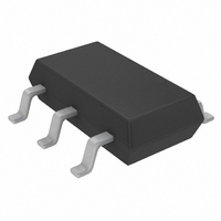
IC CTRLR LOWLOS PWRPATH TSOT23-6

LTC4412ES6#TRMPBF

Manufacturer Part Number
LTC4412ES6#TRMPBF
Description
IC CTRLR LOWLOS PWRPATH TSOT23-6
Manufacturer
Linear Technology
Series
PowerPath™r
Datasheet

Specifications of LTC4412ES6#TRMPBF

Applications
Handheld/Mobile Devices
Fet Type
P-Channel
Number Of Outputs
1
Internal Switch(s)
No
Delay Time - On
110µs
Delay Time - Off
13µs
Voltage - Supply
2.5 V ~ 28 V
Current - Supply
16µA
Operating Temperature
-40°C ~ 85°C
Mounting Type
Surface Mount
Package / Case
TSOT-23-6, TSOT-6
Lead Free Status / RoHS Status
Lead free / RoHS Compliant
Other names
LTC4412ES6#TRMPBFTR

Available stocks

Company
Part Number
Manufacturer
Quantity
Price
Company:
Part Number:
LTC4412ES6#TRMPBFLTC4412ES6
Manufacturer:
LT
Quantity:
5 321
Company:
Part Number:
LTC4412ES6#TRMPBFLTC4412ES6
Manufacturer:
LT
Quantity:
10 000
Company:
Part Number:
LTC4412ES6#TRMPBFLTC4412ES6
Manufacturer:
LT
Quantity:
20 000
Company:
Part Number:
LTC4412ES6#TRMPBFLTC4412ES6#PBF
Manufacturer:
LINEAR
Quantity:
2 000
Company:
Part Number:
LTC4412ES6#TRMPBFLTC4412ES6#PBF
Manufacturer:
LINEAR/凌特
Quantity:
20 000
PowerPath and ThinSOT are trademarks of Linear Technology Corporation.
FEATURES
TYPICAL APPLICATIO
APPLICATIO S
, LT, LTC and LTM are registered trademarks of Linear Technology Corporation.
Very Low Loss Replacement for Power Supply
OR’ing Diodes
Minimal External Components
Automatic Switching Between DC Sources
Simplifies Load Sharing with Multiple Batteries
Low Quiescent Current: 11μA
3V to 28V AC/DC Adapter Voltage Range
2.5V to 28V Battery Voltage Range
Reverse Battery Protection
Drives Almost Any Size MOSFET for Wide Range of
Current Requirements
MOSFET Gate Protection Clamp
Manual Control Input
Low Profile (1mm) ThinSOT
Cellular Phones
Notebook and Handheld Computers
Digital Cameras
USB-Powered Peripherals
Uninterruptable Power Supplies
Logic Controlled Power Switch
Figure 1. Automatic Switchover of Load Between a Battery and a Wall Adapter
ADAPTER
BATTERY
CELL(S)
INPUT
WALL
1
2
3
U
V
GND
CTL
IN
LTC4412
1N5819
SENSE
GATE
STAT
6
5
4
FDN306P
TM
Package
U
C
V
OUT
CC
470k
4412 F01
TO LOAD
STATUS OUTPUT
LOW WHEN WALL
ADAPTER PRESENT
DESCRIPTIO
The LTC
create a near ideal diode function for power switchover or
load sharing. This permits highly efficient OR’ing of mul-
tiple power sources for extended battery life and low self-
heating. When conducting, the voltage drop across the
MOSFET is typically 20mV. For applications with a wall
adapter or other auxiliary power source, the load is auto-
matically disconnected from the battery when the auxiliary
source is connected. Two or more LTC4412s may be
interconnected to allow load sharing between multiple
batteries or charging of multiple batteries from a single
charger.
The wide supply operating range supports operation from
one to six Li-Ion cells in series. The low quiescent current
(11μA typical) is independent of the load current. The gate
driver includes an internal voltage clamp for MOSFET
protection.
The STAT pin can be used to enable an auxiliary P-channel
MOSFET power switch when an auxiliary supply is
detected. This pin may also be used to indicate to a
microcontroller that an auxiliary supply is connected. The
control (CTL) input enables the user to force the primary
MOSFET off and the STAT pin low.
The LTC4412 is available in a low profile (1mm) ThinSOT
package.
®
4412 controls an external P-channel MOSFET to
Low Loss PowerPath
Controller in ThinSOT
1
0
0.02
U
LTC4412
LTC4412 vs Schottky Diode
Forward Voltage Drop
FORWARD VOLTAGE (V)
CONSTANT
CONSTANT
VOLTAGE
R
ON
SCHOTTKY
DIODE
LTC4412
4412 F01b
0.5
4412fa
1
TM

Related parts for LTC4412ES6#TRMPBF

LTC4412ES6#TRMPBF Summary of contents

Page 1

... Notebook and Handheld Computers ■ Digital Cameras ■ USB-Powered Peripherals ■ Uninterruptable Power Supplies ■ Logic Controlled Power Switch , LT, LTC and LTM are registered trademarks of Linear Technology Corporation. PowerPath and ThinSOT are trademarks of Linear Technology Corporation. U TYPICAL APPLICATIO 1N5819 WALL ADAPTER INPUT FDN306P ...

Page 2

LTC4412 ABSOLUTE MAXIMUM (Note 1) Supply Voltage (V ) .................................. –14V to 36V IN Voltage from V to SENSE ........................ – 28V to 28V IN Input Voltage CTL ........................................................– 0.3V to 36V SENSE .................................................... –14V to 36V ...

Page 3

ELECTRICAL CHARACTERISTICS temperature range, unless otherwise noted specifications are at T and current out of a pin is negative. All voltages are referenced to GND, unless otherwise specified. SYMBOL PARAMETER I Quiescent Supply Current at Low Supply QCL with CTL ...

Page 4

LTC4412 W U TYPICAL PERFOR A CE CHARACTERISTICS V vs Temperature and FR Supply Voltage 2. 28V –50 – 100 TEMPERATURE (°C) 4412 G01 I vs Temperature ...

Page 5

CTIO S V (Pin 1): Primary Input Supply Voltage. Supplies power IN to the internal circuitry and is one of two voltage sense inputs to the internal analog controller (The other input to the controller ...

Page 6

LTC4412 U OPERATIO Operation can best be understood by referring to the Block Diagram, which illustrates the internal circuit blocks along with the few external components, and the graph that accompanies Figure 1. The terms primary and auxiliary are arbitrary ...

Page 7

U U APPLICATIO S I FOR ATIO Introduction The system designer will find the LTC4412 useful in a variety of cost and space sensitive power control applica- tions that include low loss diode OR’ing, fully automatic switchover from a primary ...

Page 8

LTC4412 U U APPLICATIO S I FOR ATIO V and SENSE Pin Usage IN Since the analog controller’s thresholds are small (±20mV), the V and SENSE pin connections should be made way to avoid unwanted I • ...

Page 9

U TYPICAL APPLICATIO S Automatic PowerPath Control The applications shown in Figures 1, 2 and 3 are automatic ideal diode controllers that require no assistance from a microcontroller. Each of these will automatically connect the higher supply voltage, after accounting ...

Page 10

LTC4412 U TYPICAL APPLICATIO S This is due to the SENSE pin voltage rising above the battery voltage and turning off the MOSFET before the Schottky diode turns on. The factors that determine the magnitude of the voltage droop are ...

Page 11

... Single Charging Source Information furnished by Linear Technology Corporation is believed to be accurate and reliable. However, no responsibility is assumed for its use. Linear Technology Corporation makes no represen- tation that the interconnection of its circuits as described herein will not infringe on existing patent rights. High Side Power Switch Figure 7 illustrates an application circuit for a logic con- trolled high side power switch ...

Page 12

... Enables Simultaneous Battery Charging and Operation of USB Component Peripheral Devices www.linear.com ● 2.90 BSC (NOTE 4) PIN ONE ID 0.30 – 0.45 6 PLCS (NOTE 3) 0.01 – 0.10 1.90 BSC S6 TSOT-23 0302 REV B LT 0607 • PRINTED IN USA © LINEAR TECHNOLOGY CORPORATION 2002 4412fa ...

Related keywords