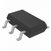
LTC4412IS6#TRMPBF Linear Technology, LTC4412IS6#TRMPBF Datasheet - Page 11

LTC4412IS6#TRMPBF
Manufacturer Part Number
LTC4412IS6#TRMPBF
Description
IC PWR PATH CNTRLR TSOT23-6
Manufacturer
Linear Technology
Series
PowerPath™r
Datasheet
1.LTC4412ES6TRMPBF.pdf
(12 pages)
Specifications of LTC4412IS6#TRMPBF
Applications
Handheld/Mobile Devices
Fet Type
P-Channel
Number Of Outputs
1
Internal Switch(s)
No
Delay Time - On
110µs
Delay Time - Off
13µs
Voltage - Supply
2.5 V ~ 28 V
Current - Supply
16µA
Operating Temperature
-40°C ~ 85°C
Mounting Type
Surface Mount
Package / Case
TSOT-23-6, TSOT-6
Operating Temperature (max)
85C
Operating Temperature (min)
-40C
Pin Count
6
Mounting
Surface Mount
Package Type
TSOT-23
Case Length
2.9mm
Screening Level
Industrial
Lead Free Status / RoHS Status
Lead free / RoHS Compliant
Other names
LTC4412IS6#TRMPBFTR
Available stocks
Company
Part Number
Manufacturer
Quantity
Price
CHARGER
Multiple Battery Charging
Figure 6 illustrates an application circuit for automatic
dual battery charging from a single charger. Whichever
battery has the lower voltage will receive the charging
current until both battery voltages are equal, then both will
be charged. When both are charged simultaneously, the
higher capacity battery will get proportionally higher cur-
rent from the charger. For Li-Ion batteries, both batteries
will achieve the float voltage minus the forward regulation
voltage of 20mV. This concept can apply to more than two
batteries. The STAT pins provide information as to which
batteries are being charged. For intelligent control, the
CTL pin input can be used with a microcontroller and
back-to-back MOSFETs as shown in Figure 4. This allows
complete control for disconnection of the charger from
either battery.
TYPICAL APPLICATIO S
BATTERY
0.1μF
INPUT
Figure 6. Automatic Dual Battery Charging
from Single Charging Source
1
2
3
1
2
3
*DRAIN-SOURCE DIODE OF MOSFET
V
GND
CTL
V
GND
CTL
LTC4412
IN
LTC4412
IN
SENSE
SENSE
GATE
GATE
STAT
STAT
6
5
4
6
5
4
*
*
Information furnished by Linear Technology Corporation is believed to be accurate and reliable.
However, no responsibility is assumed for its use. Linear Technology Corporation makes no represen-
tation that the interconnection of its circuits as described herein will not infringe on existing patent rights.
U
V
V
CC
CC
470k
470k
BAT1
BAT2
4412 F06
TO LOAD OR
PowerPath
CONTROLLER
STATUS IS HIGH
WHEN BAT1 IS
CHARGING
TO LOAD OR
PowerPath
CONTROLLER
STATUS IS HIGH
WHEN BAT2 IS
CHARGING
High Side Power Switch
Figure 7 illustrates an application circuit for a logic con-
trolled high side power switch. When the CTL pin is a
logical low, the LTC4412 will turn on the MOSFET. Be-
cause the SENSE pin is grounded, the LTC4412 will apply
maximum clamped gate drive voltage to the MOSFET.
When the CTL pin is a logical high, the LTC4412 will turn
off the MOSFET by pulling its gate voltage up to the supply
input voltage and thus deny power to the load. The
MOSFET is connected with its source connected to the
power source. This disables the drain-source diode from
supplying voltage to the load when the MOSFET is off. Note
that if the load is powered from another source, then the
drain-source diode can forward bias and deliver current to
the power supply connected to the V
Figure 7. Logic Controlled High Side Power Switch
SUPPLY
0.1μF
INPUT
LOGIC
INPUT
*DRAIN-SOURCE DIODE OF MOSFET
1
2
3
V
GND
CTL
LTC4412
IN
SENSE
GATE
STAT
P-CHANNEL
4412 F07
6
5
4
MOSFET
*
IN
pin.
LTC4412
C
OUT
TO LOAD
11
4412fa


