LTC4413EDD#PBF Linear Technology, LTC4413EDD#PBF Datasheet
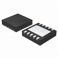
IC IDEAL DIODE DUAL 10-DFN

LTC4413EDD#PBF

Manufacturer Part Number
LTC4413EDD#PBF
Description
IC IDEAL DIODE DUAL 10-DFN
Manufacturer
Linear Technology
Datasheet

Specifications of LTC4413EDD#PBF

Applications
Handheld/Mobile Devices
Fet Type
P-Channel
Number Of Outputs
2
Internal Switch(s)
Yes
Delay Time - On
11µs
Delay Time - Off
2µs
Voltage - Supply
2.5 V ~ 5.5 V
Current - Supply
25µA
Operating Temperature
-40°C ~ 85°C
Mounting Type
Surface Mount
Package / Case
10-DFN
Input Voltage
5.5V
No. Of Outputs
2
Power Dissipation Pd
1.5W
Supply Voltage Range
2.5V To 5.5V
No. Of Pins
10
Operating Temperature Range
-40°C To +85°C
Msl
MSL 1 - Unlimited
Termination Type
SMD
Rohs Compliant
Yes
Filter Terminals
SMD
Lead Free Status / RoHS Status
Lead free / RoHS Compliant

Available stocks

Company
Part Number
Manufacturer
Quantity
Price
Company:
Part Number:
LTC4413EDD#PBF
Manufacturer:
Linear Technology
Quantity:
1 921
Company:
Part Number:
LTC4413EDD#PBF
0
Company:
Part Number:
LTC4413EDD#PBFLTC4413EDD#TRPBF
Manufacturer:
LT
Quantity:
2 008
Company:
Part Number:
LTC4413EDD#PBFLTC4413EDD#TRPBF
Manufacturer:
LINEAR/凌特
Quantity:
20 000
Company:
Part Number:
LTC4413EDD#PBFLTC4413EDD#TRPBF
0
n
n
n
n
n
n
n
n
n
n
n
n
n
APPLICATIONS
n
n
n
n
n
L, LT, LTC, LTM, Linear Technology and the Linear logo are registered trademarks of Linear
Technology Corporation. All other trademarks are the property of their respective owners.
TYPICAL APPLICATION
FEATURES
(0V TO 5.5V)
Battery and Wall Adapter Diode ORing in Handheld
Products
Backup Battery Diode ORing
Power Switching
USB Peripherals
Uninterruptable Supplies
ADAPTER
2-Channel Ideal Diode ORing or Load Sharing
Low Loss Replacement for ORing Diodes
Low Forward On-Resistance (100mΩ Max at 3.6V)
Low Reverse Leakage Current (1μA Max)
Small Regulated Forward Voltage (28mV Typ)
2.5V to 5.5V Operating Range
2.6A Maximum Forward Current
Internal Current Limit and Thermal Protection
Slow Turn-On/Off to Protect Against Inductive
Source Impedance-Induced Voltage Spiking
Ultralow Quiescent Current Consumption, Low
Power Alternative to the LTC4413-1
Status Output to Indicate if Selected Channel is
Conducting
Programmable Channel On/Off
Low Profi le (0.75mm) 10-Lead 3mm × 3mm DFN
Package
WALL
10μF
BAT
ENBA
GND
ENBB
INB
INA
CONTROL CIRCUIT
LTC4413
OUTB
OUTA
STAT
V
CC
470k
4.7μF
4413 TA01
STAT IS HIGH WHEN
BAT IS SUPPLYING
LOAD CURRENT
TO LOAD
Ideal Diodes in 3mm × 3mm DFN
DESCRIPTION
The LTC
each capable of supplying up to 2.6A from input voltages
between 2.5V and 5.5V. Each ideal diode uses a 100mΩ
P-channel MOSFET that independently connects INA to
OUTA and INB to OUTB. During normal forward operation
the voltage drop across each of these diodes is regulated
to as low as 28mV. Quiescent current is less than 40μA
for diode currents up to 1A. If either of the output voltages
exceeds its respective input voltages, that MOSFET is
turned off and less than 1μA of reverse current will fl ow
from OUT to IN. Maximum forward current in each MOSFET
is limited to a constant 2.6A and internal thermal limiting
circuits protect the part during fault conditions.
Two active-high control pins independently turn off the
two ideal diodes contained within the LTC4413, control-
ling the operation mode as described by Table 1. When
the selected channel is reverse biased, or the LTC4413 is
put into low power standby, a status signal indicates this
condition with a low voltage.
A 9μA open-drain STAT pin is used to indicate conduction
status. When terminated to a positive supply through a
470k resistor, the STAT pin can be used to indicate that the
selected diode is conducting with a high voltage. This signal
can also be used to drive an auxiliary P-channel MOSFET
power switch to control a third alternate power source
when the LTC4413 is not conducting forward current.
The LTC4413 is housed in a 10-lead DFN package.
Dual 2.6A, 2.5V to 5.5V,
®
4413 contains two monolithic ideal diodes,
2000
1500
1000
500
0
0
LTC4413 vs 1N5817 Schottky
LTC4413
100
V
FWD
200
(mV)
300
1N5817
4413 TA01b
LTC4413
400
4413fc
1

Related parts for LTC4413EDD#PBF

LTC4413EDD#PBF Summary of contents

Page 1

... Backup Battery Diode ORing n Power Switching n USB Peripherals n Uninterruptable Supplies L, LT, LTC, LTM, Linear Technology and the Linear logo are registered trademarks of Linear Technology Corporation. All other trademarks are the property of their respective owners. TYPICAL APPLICATION ENBA GND LTC4413 ENBB STAT ...

Page 2

... Above 70°C) .........................1500mW ORDER INFORMATION LEAD FREE FINISH TAPE AND REEL LTC4413EDD#PBF LTC4413EDD#TRPBF Consult LTC Marketing for parts specifi ed with wider operating temperature ranges. Consult LTC Marketing for information on non-standard lead based fi nish parts. For more information on lead free part marking, go to: For more information on tape and reel specifi ...

Page 3

... ENBHYST I ENB Inputs Pull-Down Current ENB PowerPath is a trademark of Linear Technology Corporation. Note 1: Stresses beyond those listed under Absolute Maximum Ratings may cause permanent damage to the device. Exposure to any Absolute Maximum Rating condition for extended periods may affect device reliability and lifetime. ...

Page 4

LTC4413 TYPICAL PERFORMANCE CHARACTERISTICS LOAD 200 120°C 80°C 40°C 160 0°C –40°C 120 100E-6 1E-3 10E-3 100E-3 1E+0 10E+0 I (A) LOAD 4413 G01 I vs Temperature (V = 3.5V ...

Page 5

TYPICAL PERFORMANCE CHARACTERISTICS V and FWD FWD LOAD 300 120°C V 80°C FWD 250 40°C 0°C –40°C 200 R FWD 150 100 100 1000 10000 I (mA) LOAD 4413 G09 ENB Turn-On, 240μs ...

Page 6

LTC4413 TYPICAL PERFORMANCE CHARACTERISTICS – LEAK REVERSE 10E-6 80°C 40°C 0°C –40°C 1E-6 100E-9 10E-9 1E (V) REVERSE 4413 G16 PIN FUNCTIONS INA (Pin 1): Primary Ideal Diode Anode and ...

Page 7

BLOCK DIAGRAM INA 1 OVER CURRENT – O.5V ENBA + 2 3μA GND 3 INB 5 OVER CURRENT – O.5V ENBB + 4 3μA PA – + – UVLO + OUTA (MAX) OUTB (MAX) V GATEA – OFF ...

Page 8

LTC4413 OPERATION The LTC4413 is described with the aid of the Block Diagram (Figure 1). Operation begins when the power source rises above the undervoltage lockout (UVLO) INA INB voltage of 2.4V and either of the ...

Page 9

OPERATION For short durations after the output is shorted, the current may exceed I . The magnitude of this peak MAX short-circuit current can be large, depending on the load current immediately before the short circuit occurs. During overcurrent operation, ...

Page 10

LTC4413 APPLICATIONS INFORMATION MP1 FDR8508 WALL ADAPTER C1 10μF R1 1000k 2 ENBA 4 R2 ENBB STAT 200k 3,11 GND LTC4413 IDEAL 1 INA OUTA BATA 1-CELL Li-Ion IDEAL 5 INB OUTB BATB 1-CELL Li-Ion C1:C1206C106K8PAC C2:C1206C475K8PAC Figure 3 batteries ...

Page 11

... ADAPTER Information furnished by Linear Technology Corporation is believed to be accurate and reliable. However, no responsibility is assumed for its use. Linear Technology Corporation makes no representa- tion that the interconnection of its circuits as described herein will not infringe on existing patent rights. until both battery voltages are equal, then both are charged. ...

Page 12

... Low Loss Ideal Diode in ThinSOT Load Sharing LTC4412/LTC4412HV PowerPath Controllers in ThinSOT LTC4413-1/LTC4413-2 Dual 2.6A, 2.5V to 5.5V Fast Ideal Diodes in 3mm × 3mm DFN ThinSOT is a trademark of Linear Technology Corporation. Linear Technology Corporation 12 1630 McCarthy Blvd., Milpitas, CA 95035-7417 (408) 432-1900 FAX: (408) 434-0507 ● ...

Related keywords