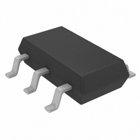
LTC4412HVIS6#TRM Linear Technology, LTC4412HVIS6#TRM Datasheet - Page 8

LTC4412HVIS6#TRM
Manufacturer Part Number
LTC4412HVIS6#TRM
Description
IC CONTROLLER LOW LOSS TSOT23-6
Manufacturer
Linear Technology
Series
PowerPath™r
Datasheet
1.LTC4412HVIS6TR.pdf
(12 pages)
Specifications of LTC4412HVIS6#TRM
Applications
Handheld/Mobile Devices
Fet Type
P-Channel
Number Of Outputs
1
Internal Switch(s)
No
Delay Time - On
110µs
Delay Time - Off
13µs
Voltage - Supply
2.5 V ~ 36 V
Current - Supply
19µA
Operating Temperature
-40°C ~ 125°C
Mounting Type
Surface Mount
Package / Case
TSOT-23-6, TSOT-6
Lead Free Status / RoHS Status
Contains lead / RoHS non-compliant
Other names
LTC4412HVIS6
LTC4412HVIS6
LTC4412HVIS6
Available stocks
Company
Part Number
Manufacturer
Quantity
Price
LTC4412HV
APPLICATIO S I FOR ATIO
V
Since the analog controller’s thresholds are small ( 20mV),
the V
way to avoid unwanted I • R drops in the power path. Both
pins are protected from negative voltages.
GATE Pin Usage
The GATE pin controls the external P-channel MOSFET
connected between the V
current is supplied by the power source at V
mode of operation, the internal current source, which is
responsible for pulling the GATE pin up, is limited to a few
microamps (I
rents exceed this, the GATE pin voltage will reach the
clamp voltage (V
current sink, which is responsible for pulling the GATE pin
down, has a higher current capability (I
auxiliary supply input pulling up on the SENSE pin and
exceeding the V
enters the reverse turn-off mode and a much stronger
current source is available to oppose external leakage
currents and turn off the MOSFET (V
While in forward regulation, if the on resistance of the
MOSFET is too high to maintain forward regulation, the
GATE pin will maximize the MOSFET’s V
clamp voltage (V
between the higher of V
Status Pin Usage
During normal operation, the open-drain STAT pin can be
biased at any voltage between ground and 36V regardless
of the supply voltage to the LTC4412HV. It is usually
connected to a resistor whose other end connects to a
voltage source. In the forward regulation mode, the STAT
pin will be open (I
other auxiliary supply is connected to that input, and the
voltage on SENSE is higher than V
system is in the reverse turn-off mode. During this mode
of operation the STAT pin will sink 10 A of current
(I
resistor, depending on the resistance, which is useful to
turn on an auxiliary P-channel MOSFET or signal to a
microcontroller that an auxiliary power source is con-
8
IN
S(SNK)
and SENSE Pin Usage
IN
and SENSE pin connections should be made in a
). This will result in a voltage change across the
G(SRC)
IN
GON
GON
pin voltage by 20mV (V
S(OFF)
U
). If external opposing leakage cur-
) and V
). The clamping action takes place
IN
). When a wall adaptor input or
IN
U
or V
and SENSE pins when the load
DS
will be smaller. The internal
SENSE
IN
W
GOFF
and the GATE pin.
+ 20mV (V
G(SNK)
GS
RTO
).
to that of the
), the device
U
). With an
IN
RTO
. In this
), the
nected. External leakage currents, if significant, should be
accounted for when determining the voltage across the
resistor when the STAT pin is either on or off.
Control Pin Usage
This is a digital control input pin with low threshold
voltages (V
as 1V. During normal operation, the CTL pin can be biased
at any voltage between ground and 36V, regardless of the
supply voltage to the LTC4412HV. A logical high input on
this pin forces the gate to source voltage of the primary
P-channel MOSFET power switch to a small voltage (V
This will turn the MOSFET off and no current will flow from
the primary power input at V
so that the drain to source diode is not forward biased. The
high input also forces the STAT pin to sink 10 A of current
(I
amples on using the STAT pin. A 3.5 A internal pull-down
current (I
input if the pin should be open.
Protection
Most of the application circuits shown provide some
protection against supply faults such as shorted, low or
reversed supply inputs. The fault protection does not
protect shorted supplies but can isolate other supplies and
the load from faults. A necessary condition of this protec-
tion is for all components to have sufficient breakdown
voltages. In some cases, if protection of the auxiliary input
(sometimes referred to as the wall adapter input) is not
required, then the series diode or MOSFET may be elimi-
nated.
Internal protection for the LTC4412HV is provided to
prevent damaging pin currents and excessive internal self
heating during a fault condition. These fault conditions can
be a result of any LTC4412HV pins shorted to ground or to
a power source that is within the pin’s absolute maximum
voltage limits. Both the V
being taken significantly below ground without current
drain or damage to the IC (see Absolute Maximum Voltage
Limits). This feature allows for reverse-battery condition
without current drain or damage. This internal protection
is not designed to prevent overcurrent or overheating of
external components.
S(SNK)
). See the Typical Applications for various ex-
CTL
IL,
) on the CTL pin will insure a logical low level
V
IH
) for use with logic powered from as little
IN
and SENSE pins are capable of
IN
if the MOSFET is configured
sn4412hv 4412hvfs
GOFF
).


