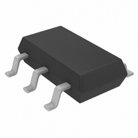
LTC4412HVIS6#TRMPBF Linear Technology, LTC4412HVIS6#TRMPBF Datasheet - Page 6

LTC4412HVIS6#TRMPBF
Manufacturer Part Number
LTC4412HVIS6#TRMPBF
Description
IC CTRLR LOWLOS PWRPATH TSOT23-6
Manufacturer
Linear Technology
Series
PowerPath™r
Datasheet
1.LTC4412HVIS6TR.pdf
(12 pages)
Specifications of LTC4412HVIS6#TRMPBF
Applications
Handheld/Mobile Devices
Fet Type
P-Channel
Number Of Outputs
1
Internal Switch(s)
No
Delay Time - On
110µs
Delay Time - Off
13µs
Voltage - Supply
2.5 V ~ 36 V
Current - Supply
19µA
Operating Temperature
-40°C ~ 125°C
Mounting Type
Surface Mount
Package / Case
TSOT-23-6, TSOT-6
Lead Free Status / RoHS Status
Lead free / RoHS Compliant
Available stocks
Company
Part Number
Manufacturer
Quantity
Price
LTC4412HV
OPERATIO
6
Operation can best be understood by referring to the Block
Diagram, which illustrates the internal circuit blocks along
with the few external components, and the graph that
accompanies Figure 1. The terms primary and auxiliary are
arbitrary and may be changed to suit the application.
Operation begins when either or both power sources are
applied and the CTL control pin is below the input low
voltage of 0.35V (V
present, the Power Source Selector will power the
LTC4412HV from the V
current to the Analog Controller block that is proportional
to the voltage difference in the V
the voltage on SENSE is lower than V
Analog Controller will instruct the Linear Gate Driver and
Voltage Clamp block to pull down the GATE pin voltage and
turn on the external P-channel MOSFET. The dynamic pull-
down current of 50 A (I
voltage reaches ground or the gate clamp voltage. The
gate clamp voltage is 7V (V
or V
the LTC4412HV will regulate the GATE voltage to maintain
a 20mV difference between V
the V
regulation mode and the load will be powered from the
primary supply. As the load current varies, the GATE
voltage will be controlled to maintain the 20mV difference.
If the load current exceeds the P-channel MOSFET’s ability
to deliver the current with a 20mV V
will clamp, the MOSFET will behave as a fixed resistor and
the forward voltage will increase slightly. While the MOSFET
is on the STAT pin is an open circuit.
When an auxiliary supply is applied, the SENSE pin will be
pulled higher than the V
SENSE
DS
of the MOSFET. The system is now in the forward
. As the SENSE voltage pulls up to V
U
IL
). If only the primary supply is
IN
IN
pin through the external diode.
pin. Amplifier A1 will deliver a
G(SNK)
G(ON)
IN
IN
and V
) below the higher of V
) stops when the GATE
and SENSE pins. While
DS
IN
SENSE
– 20mV (V
the GATE voltage
which is also
IN
– 20mV,
FR
), the
IN
The Power Source Selector will power the LTC4412HV
from the SENSE pin. As the SENSE voltage pulls above
V
Gate Driver and Voltage Clamp block to pull the GATE
voltage up to turn off the P-channel MOSFET. When the
voltage on SENSE is higher than V
Analog Controller will instruct the Linear Gate Driver and
Voltage Clamp block to rapidly pull the GATE pin voltage
to the SENSE pin voltage. This action will quickly finish
turning off the external P-channel MOSFET if it hasn’t
already turned completely off. For a clean transistion, the
reverse turn-off threshold has hysteresis to prevent
uncertainty. The system is now in the reverse turn-off
mode. Power to the load is being delivered through the
external diode and no current is drawn from the primary
supply. The external diode provides protection in case
the auxiliary supply is below the primary supply, sinks
current to ground or is connected reverse polarity. Dur-
ing the reverse turn-off mode of operation the STAT pin
will sink 10 A of current (I
the external MOSFET is wired so that the drain to source
diode will momentarily forward bias when power is first
applied to V
auxiliary supply is applied.
When the CTL (control) input is asserted high, the external
MOSFET will have its gate to source voltage forced to a
small voltage V
current if connected. This feature is useful to allow control
input switching of the load between two power sources as
shown in Figure 4 or as a switchable high side driver as
shown in Figure 7. A 3.5 A internal pull- down current
(I
should become open.
IN
CTL
– 20mV, the Analog Controller will instruct the Linear
) on the CTL pin will insure a low level input if the pin
IN
and will become reverse biased when an
G(OFF)
and the STAT pin will sink 10 A of
S(SNK)
) if connected. Note that
IN
+ 20mV (V
sn4412hv 4412hvfs
RTO
), the


