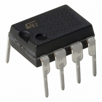
L6561 STMicroelectronics, L6561 Datasheet

L6561
Specifications of L6561
Available stocks
Related parts for L6561
L6561 Summary of contents
Page 1
... TOTEM POLE OUTPUT CURRENT: ±400mA DIP-8/SO-8 PACKAGES 2 DESCRIPTION L6561 is the improved version of the L6560 stan- dard Power Factor Corrector. Fully compatible with the standard version, it has a superior perfor- mant multiplier making the device capable of work- ing in wide input voltage range applications (from 85V to 265V) with an excellent THD ...
Page 2
... L6561 Table 2. Absolute Maximum Ratings Symbol Pin Vcc Output Totem Pole Peak Current ( INV, COMP Analog Inputs & Outputs MULT CS 4 Current Sense Input ZCD 5 Zero Current Detector P Power Dissipation @T tot T Junction Temperature Operating Range j T Storage Temperature stg Figure 3. Pin Connection (Top view) Table 3 ...
Page 3
... COMP INV I = 0.5mA SOURCE I = 0.5mA Sink V = from 0V to 0.5V MULT V = Upper Clamp Voltage COMP MULT COMP V = 2.5V MULT V = Upper Clamp Voltage COMP (1) ( ZCD I = 3mA ZCD L6561 Min. Typ. Max. Unit 8.7 9.5 10.3 V 2.2 2 5.5 mA 1.4 2.1 mA 1.4 2.1 mA ...
Page 4
... Since the current through R2 does not change, I error amplifier. This current is monitored inside the L6561 and when reaches about 37 A the output voltage of the multi- plier is forced to decrease, thus reducing the energy drawn from the mains. If the current exceeds 40 A, the OVP protection is triggered (Dynamic OVP), and the external power transistor is switched off until the current falls approximately below 10 A ...
Page 5
... Releasing the ZCD pin the internal start-up timer will restart the device. Figure 4. V OUT nominal I SC E/A OUTPUT DYNAMIC OVP STATIC OVP Figure 5. Overvoltage Protection Circuit + D97IN591 OVER VOLTAGE 2.25V Ccomp E 2.25V L6561 D97IN592A PWM DRIVER 5/13 ...
Page 6
... D2 1N5248B R1 68K R9 (*) 5 8 1.82M L6561 R10 10K 10nF 25V C6 R3 (*) R2 D3 1N4150 240K 100 12nF D2 1N5248B R1 68K R9 (*) 5 8 1.24M L6561 R10 22 F 10nF 10K 25V D1 BYT03-400 T R7 (*) 950K C3 680nF MOS 7 STP7NA40 (*) R8 0.31 10K 1W 1% D97IN549B D1 BYT13-600 T R7 (*) 998K ...
Page 7
... Boost Inductor Spec (ITACOIL E2543/E) E25x13x7 core, 3C85 ferrite 1.5 mm gap for 0.7 mH primary inductance Primary: 105 turns 20x0.1 mm Secondary: 11 turns 0.1mm Figure 10. EVAL6561-80: PCB and Component Layout (Top view, real size 57x108mm) Table 6. EVAL6561-80: Evaluation Results. V (Vac) V (Vdc) Pin (W) ...
Page 8
... L6561 Figure 11. OVP Current Threshold vs. Temperature I OVP ( -50 - Figure 12. Undervoltage Lockout Threshold vs. Temperature V CC-ON ( CC-OFF ( - (˚C) 8/13 Figure 13. Supply Current vs. Supply D94IN047A I CC (mA 0.5 0.1 0.05 0.01 0.005 0 75 100 125 T (˚C) Figure 14. Voltage Feedback Input Threshold D94IN044A 75 100 125 Voltage 1nF f = 70KHz 25˚ ...
Page 9
... SINK 1.4 1.2 1.0 0.8 0.6 0.4 0.2 0 400 I GD (mA) 0 0.5 1.0 1.5 2.0 2.5 3.0 3.5 4.0 4.5 D94IN053 SOURCE 400 I GD (mA) Family V COMP D97IN555A 3.5 5.0 4.0 3.2 3.0 2.8 2.6 V (pin3) (V) MULT L6561 (pin2) (V) 9/13 ...
Page 10
... L6561 Figure 18. DIP-8 Mechanical Data & Package Dimensions mm DIM. MIN. TYP. MAX. A 3.32 a1 0.51 B 1.15 1.65 b 0.356 0.55 b1 0.204 0.304 D 10.92 E 7.95 9.75 e 2.54 e3 7.62 e4 7.62 F 6.6 I 5.08 L 3.18 3.81 Z 1.52 10/13 inch MIN. TYP. MAX. 0.131 0.020 0.045 0.065 0.014 ...
Page 11
... Mold flash, potrusions or gate burrs shall not exceed 0.15mm (.006inch) in total (both side). inch MIN. TYP. MAX. 0.053 0.069 0.004 0.010 0.043 0.065 0.013 0.020 0.007 0.010 0.189 0.197 0.15 0.157 0.050 0.228 0.244 0.010 0.020 0.016 0.050 0.004 OUTLINE AND MECHANICAL DATA SO-8 0016023 C L6561 11/13 ...
Page 12
... L6561 Table 7. Revision History Date Revision January 2004 June 2004 12/13 15 First Issue 16 Modified the Style-look in compliance with the “Corporate Technical Publications Design Guide”. Changed input of the power amplifier connected to Multiplier (Fig. 2). Description of Changes ...
Page 13
... Australia - Belgium - Brazil - Canada - China - Czech Republic - Finland - France - Germany - Hong Kong - India - Israel - Italy - Japan - Malaysia - Malta - Morocco - Singapore - Spain - Sweden - Switzerland - United Kingdom - United States All other names are the property of their respective owners © 2004 STMicroelectronics - All rights reserved STMicroelectronics GROUP OF COMPANIES www.st.com L6561 13/13 ...


