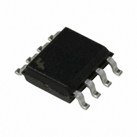
FAN7930M Fairchild Semiconductor, FAN7930M Datasheet - Page 11

FAN7930M
Manufacturer Part Number
FAN7930M
Description
IC POWER FACTOR CORR CTRLR 8SOIC
Manufacturer
Fairchild Semiconductor
Datasheet
1.FAN7930M.pdf
(22 pages)
Specifications of FAN7930M
Mode
Critical Conduction (CRM)
Current - Startup
120µA
Voltage - Supply
13 V ~ 20 V
Operating Temperature
-40°C ~ 125°C
Mounting Type
Surface Mount
Package / Case
8-SOIC (3.9mm Width)
Switching Frequency
300 KHz
Maximum Power Dissipation
195 W
Maximum Operating Temperature
+ 125 C
Mounting Style
SMD/SMT
Minimum Operating Temperature
- 40 C
Lead Free Status / RoHS Status
Lead free / RoHS Compliant
Frequency - Switching
-
Lead Free Status / Rohs Status
Lead free / RoHS Compliant
Available stocks
Company
Part Number
Manufacturer
Quantity
Price
Part Number:
FAN7930M
Manufacturer:
FAIRCHILD/仙童
Quantity:
20 000
© 2010 Fairchild Semiconductor Corporation
FAN7930 • Rev. 1.0.1
Applications Information
1. Startup: Normally, supply voltage (V
block is fed from the additional power supply, which can
be called standby power. Without this standby power,
auxiliary winding to detect zero current detection can be
used as a supply source. Once the supply voltage of the
PFC block exceeds 12V, internal operation is enabled
until the voltage drops to 8.5V. If V
current is sinking from V
2. INV Block: Scaled-down voltage from the output is
the input for the INV pin. Many functions are embedded
based on the INV pin: transconductance amplifier,
output OVP comparator, disable comparator, and output
UVLO comparator.
For the output voltage control, a transconductance
amplifier is used instead of the conventional voltage
amplifier. The transconductance amplifier (voltage-
controlled current source) aids the implementation of
OVP and disable function. The output current of the
amplifier changes according to the voltage difference of
the inverting and non-inverting input of the amplifier. To
cancel down the line input voltage effect on power factor
correction, effective control response of PFC block
should be slower than the line frequency and this
conflicts with the transient response of controller. Two-
pole one-zero type compensation may be used to meet
both requirements.
The OVP comparator shuts down the output drive block
when the voltage of the INV pin is higher than 2.675V
and there is 0.175V hysteresis. The disable comparator
disables the operation when the voltage of the inverting
input is lower than 0.35V and there is 100mV hysteresis.
An external small-signal MOSFET can be used to
disable the IC, as shown in Figure 23. The IC operating
current decreases to reduce power consumption if the
IC is disabled. Figure 24 is the timing chart of the
internal circuit near the INV pin when rated PFC output
voltage is assumed at 390V
15V.
Figure 22.
CC
.
Startup Circuit
DC
and V
CC
CC
exceeds V
supply voltage is
CC
) of a PFC
Z
, 20mA
11
3. RDY Output: When the INV voltage is higher than
2.24V, output UVLO voltage is triggered to high and
lasts until the INV voltage is lower than 1.64V. This
signal outputs through the RDY pin. RDY pin output is
open-drain type, so needs an external pull-up resistor to
supply the proper power source. The RDY pin output
remains floating until V
Disable
I
V
OVP
OUT
V
V
V
RDY
OUT
CC
INV
2.50V
COMP
390Vdc
2.0V
PFC
0.45V
70V
Vcc<2V, internal logic is not alive.
- RDY pin is floating, so pull up voltage is shown.
- Internal signals are unknown.
Figure 24.
Figure 23.
15V
Current sourcing
2.24V
349V
Timing Chart for INV Block
Circuit Around INV Pin
CC
Voltage is decided by pull-up voltage.
is higher than 2V.
2.65V
413V
I sinking
2.50V
390V
Current sourcing
www.fairchildsemi.com
256V
1.64V
55V
0.35V
t


