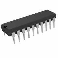
LT1509IN Linear Technology, LT1509IN Datasheet - Page 7

LT1509IN
Manufacturer Part Number
LT1509IN
Description
IC PFC CTRLR AVERAGE CURR 20DIP
Manufacturer
Linear Technology
Datasheet
1.LT1509CN.pdf
(16 pages)
Specifications of LT1509IN
Mode
Average Current
Frequency - Switching
100kHz
Voltage - Supply
27V
Operating Temperature
-40°C ~ 125°C
Mounting Type
Through Hole
Package / Case
20-DIP (0.300", 7.62mm)
Lead Free Status / RoHS Status
Contains lead / RoHS non-compliant
Current - Startup
-
Available stocks
Company
Part Number
Manufacturer
Quantity
Price
Part Number:
LT1509IN#PBF
Manufacturer:
LINEAR/凌特
Quantity:
20 000
APPLICATIONS
R
oscillator charging current and the maximum multiplier
output current which is used to limit the maximum line
current.
SS1 (Pin 16): Soft Start. SS1 is reset to zero for low V
When V
to ramp up at a rate set by the internal 12 A current source
and an external capacitor. During this ramp up, PFC
reference voltage is equal to SS1 voltage. After SS1 rises
past 7.5V, reference voltage remains at 7.5V.
V
has two fast gate drivers required to fast charge high
power MOSFET gate capacitances. Good supply bypass-
ing is required consisting of a 0.1 F ceramic capacitor in
parallel with a low ESR electrolytic capacitor (56 F or
higher) in close proximity to IC GND.
Voltage Error Amplifier (PFC Section)
The voltage error amplifier has a 100dB DC gain and 3MHz
unity-gain frequency. The output is internally clamped at
13.3V with V
decreases to V
noninverting input is tied to the 7.5V
and can be pulled down with the SS1 pin. Referring to
Figure 1, V
R2 = 20k, V
compensation for the voltage loop. Gain of the voltage
error amp with the values shown is given by:
The small-signal gain for the remaining portion of the
voltage loop for frequencies below the current loop band-
width is (see Figure 2):
PIN
SET
CC
I
VA
VA
U
M(MAX)
V
V
(Pin 17): This is the supply for the chip. The LT1509
OUT
OUT
(Pin 15): A resistor from R
OUT
OUT
FUNCTIONS
CC
rises above lockout threshold, SS1 is released
= 3.75V/R
= –
=
OUT
U
OUT
CC
(5
= 382V. R1 through R4, C1 and C2 form the
= V
= 18V. Maximum error amp output voltage
(j)(f)(6.6)
CC
j)(f)(C
REF
U
– 1.5V for V
SET
U
[(R1 + R2)/R2]. With R1 = 1M and
1 + j
V
IN
OUT
INFORMATION
U
1 + j
1
f
(For application help with the PFC portion of this chip, see the LT1248 data sheet)
)(V
11
OUT
f
CC
SET
W
)
less than 12V. The
REF
to GND sets the
R
through a diode
(R
S
(R
REF
IAC
U
)(P
+ 25k)
IN
)
CC
.
With V
R
85/(j)(f). At very low frequencies, the loop has a – 40dB/
decade slope. Additional zero-pole compensation is added
at 1Hz and 11Hz. The resulting loop gain and phase margin
is shown in Figure 3. The unity-gain bandwidth is low
compared to 120Hz, which results in low distortion and a
high power factor.
PWM SECTION
SS2 (Pin 13): PWM Soft Start. The comparator PWMOK
monitors the OVP pin and releases the SS2 after the PFC
output gets close to the final voltage.
V
connects to the optocoupler amplifier output. A pull-up
current of 50 A flows out of the pin.
RAMP (Pin 19): PWM current mode current sense input
with current limit set to 1V.
GTDR2 (Pin 20): The PWM MOSFET gate driver is a 1.5A
fast totem pole output. It is clamped at 15V. Capacitive
loads like the MOSFET gates may cause overshoot. A gate
series resistor of at least 5 will prevent the overshoot.
C
IAC
REGULATOR OUTPUT
(Pin 18): PWM current mode control voltage. Normally
V
= 1M, V
OUT
IN
= 382V
= 120VAC, P
R1
1M
R2
20k
OUT
20k
R3
= 382V and C
V
OVP
SENSE
IN
= 150W, R
V
Figure 1
REF
1.05V
= 7.5V
REF
OUT
–
+
–
+
0.047 F
0.47 F
= 470 F, V
C2
C1
ERROR AMP
OVERVOLTAGE
COMPARATOR
S
= 0.15 , R
330k
R4
VA
OUT
LT1509
LT1509
OUT
LT1509 • F01
/VA
REF
OUT
= 4k,
7
=


