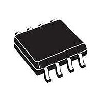
TEA1791AT/N1,118 NXP Semiconductors, TEA1791AT/N1,118 Datasheet - Page 3

TEA1791AT/N1,118
Manufacturer Part Number
TEA1791AT/N1,118
Description
IC CTLR SYNC RECTIFIER 8SOIC
Manufacturer
NXP Semiconductors
Series
GreenChip™r
Datasheet
1.TEA1791ATN1118.pdf
(13 pages)
Specifications of TEA1791AT/N1,118
Package / Case
*
Mounting Type
*
Voltage - Supply
8.5 V ~ 38 V
Operating Temperature
-20°C ~ 150°C
Mode
Discontinuous Conduction (DCM)
Input / Supply Voltage (max)
38 V
Input / Supply Voltage (min)
8.5 V
Supply Current
0.95 mA
Operating Temperature Range
- 40 C to + 150 C
Mounting Style
SMD/SMT
Maximum Operating Temperature
+ 150 C
Minimum Operating Temperature
- 40 C
Output Current
3 A
Lead Free Status / RoHS Status
Lead free / RoHS Compliant
Frequency - Switching
-
Current - Startup
-
Lead Free Status / Rohs Status
Lead free / RoHS Compliant
Other names
935290157118
Available stocks
Company
Part Number
Manufacturer
Quantity
Price
Part Number:
TEA1791AT/N1,118
Manufacturer:
NXP/恩智浦
Quantity:
20 000
NXP Semiconductors
7. Functional description
TEA1791AT
Product data sheet
7.1 Introduction
7.2 Start-up and UnderVoltage LockOut (UVLO)
7.3 Synchronous rectification
The TEA1791AT is the controller for synchronous rectification to be used in discontinuous
conduction mode and quasi-resonant flyback converters.
The IC leaves the undervoltage lockout state and activates the synchronous rectifier
circuitry as soon as the voltage on the V
voltage drops below 8.0 V (typical), the undervoltage lockout state is reentered and the
SR driver output is actively kept low.
After a negative voltage (−310 mV typical) is sensed on the SRSENSE pin, the driver
output voltage is driven HIGH and the external MOSFET is switched on. As soon as the
SRSENSE voltage rises to −55 mV the driver output voltage is regulated to maintain the
−55 mV on the SRSENSE pin. As soon as the SRSENSE voltage is above −12 mV, the
driver output is pulled to ground.
When the SR MOSFET is switched on, the input signal on the SRSENSE pin is blanked
for 0.93 μs (typical). This eliminates false switch-off due to high frequency at the start of
the secondary stroke.
Because the driver output voltage is reduced as soon as the voltage on the SRSENSE pin
is −55 mV, the external power switch can be switched off quickly when the current through
the switch reaches zero. With this zero current switch-off, no separate Standby mode is
needed to maintain high efficiency during the no-load operation. The zero current is
detected by sensing a −12 mV level on the SRSENSE pin (see
All information provided in this document is subject to legal disclaimers.
Rev. 01 — 7 June 2010
CC
GreenChip synchronous rectifier controller
pin is above 8.5 V (typical). As soon as the
Figure
TEA1791AT
3).
© NXP B.V. 2010. All rights reserved.
3 of 13


