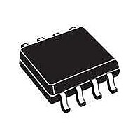
TEA1791AT/N1,118 NXP Semiconductors, TEA1791AT/N1,118 Datasheet - Page 4

TEA1791AT/N1,118
Manufacturer Part Number
TEA1791AT/N1,118
Description
IC CTLR SYNC RECTIFIER 8SOIC
Manufacturer
NXP Semiconductors
Series
GreenChip™r
Datasheet
1.TEA1791ATN1118.pdf
(13 pages)
Specifications of TEA1791AT/N1,118
Package / Case
*
Mounting Type
*
Voltage - Supply
8.5 V ~ 38 V
Operating Temperature
-20°C ~ 150°C
Mode
Discontinuous Conduction (DCM)
Input / Supply Voltage (max)
38 V
Input / Supply Voltage (min)
8.5 V
Supply Current
0.95 mA
Operating Temperature Range
- 40 C to + 150 C
Mounting Style
SMD/SMT
Maximum Operating Temperature
+ 150 C
Minimum Operating Temperature
- 40 C
Output Current
3 A
Lead Free Status / RoHS Status
Lead free / RoHS Compliant
Frequency - Switching
-
Current - Startup
-
Lead Free Status / Rohs Status
Lead free / RoHS Compliant
Other names
935290157118
Available stocks
Company
Part Number
Manufacturer
Quantity
Price
Part Number:
TEA1791AT/N1,118
Manufacturer:
NXP/恩智浦
Quantity:
20 000
NXP Semiconductors
TEA1791AT
Product data sheet
7.4 Supply management
7.5 Driver
If the secondary stroke of the flyback converter is shorter than 0.93 μs (typical), the driver
output is disabled. This will guarantee stable operation for very low duty cycles. When the
secondary stroke increases above 0.99 μs (typical), the driver output is again enabled.
All internal reference voltages are derived from a temperature compensated, on-chip
band gap circuit.
The driver circuit to the gate of the external power MOSFET has a typical source
capability of 250 mA and a typical sink capability of 2.7 A. This permits fast turn-on and
turn-off of the power MOSFET for efficient operation. The source stage is coupled to the
timer (see
small current (typical 5 mA) capable of keeping the driver output voltage at its level.
Typically, the time the driver source stage delivers the 250 mA is 100 ns shorter than the
minimum synchronous rectification active time (t
is limited to 10 V (typical). This high output voltage will drive all MOSFET brands to the
minimum on-state resistance.
During start-up conditions (V
voltage is actively pulled low.
Fig 3.
Secondary
V
SRSENSE
V
Primary
DRIVER
current
current
Synchronous rectification signals
Figure
All information provided in this document is subject to legal disclaimers.
1). When the timer has finished, the source capability is reduced to a
Rev. 01 — 7 June 2010
CC
< V
startup
) and undervoltage lockout the driver output
GreenChip synchronous rectifier controller
act(sr)(min)
).The output voltage of the driver
TEA1791AT
© NXP B.V. 2010. All rights reserved.
014aaa057
0 V
−12 mV
−55 mV
−310 mV
0 A
0 A
0 V
4 of 13


