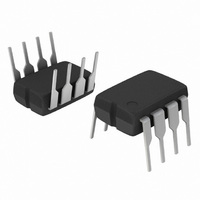
NCP1606APG ON Semiconductor, NCP1606APG Datasheet

NCP1606APG
Specifications of NCP1606APG
Available stocks
Related parts for NCP1606APG
NCP1606APG Summary of contents
Page 1
NCP1606 Cost Effective Power Factor Controller The NCP1606 is an active power factor controller specifically designed for use as a pre−converter in electronic ballasts, ac−dc adapters and other medium power off line converters (typically up to 300 W). It embeds ...
Page 2
Shutdown V OUT nPOK + R C OUT1 BULK FB E/A ESD R OUT2 D BOOST + 2 COMP V CONTROL Control ESD BOOST 270 mA Ct ESD Ct CS ESD R SENSE V DD ...
Page 3
PIN FUNCTION DESCRIPTION Pin Number Name 1 Feedback (FB) The FB pin makes available the inverting input of the internal error amplifier. A simple resistor divider scales and delivers the output voltage to the FB pin to maintain regulation. The ...
Page 4
ELECTRICAL C HARACTERISTICS (Unless otherwise specified: For typical values nF nF Control = open, ZCD = open) Symbol V UNDERVOLTAGE LOCKOUT SECTION Startup Threshold (Undervoltage Lockout Threshold, Vcc ...
Page 5
ELECTRICAL C HARACTERISTICS (Unless otherwise specified: For typical values nF nF Control = open, ZCD = open) Symbol V Negative Active Clamp Voltage @ I CL(NEG) I Current Capability of the ...
Page 6
TEMPERATURE (°C) Figure 3. Oscillator Charge Current (I vs. Temperature 3.30 3.25 3.20 3.15 3.10 3.05 3.00 −50 − TEMPERATURE (°C) Figure ...
Page 7
I 40 OVP OVP(HYS −50 − TEMPERATURE (°C) Figure 9. Overvoltage Activation Current vs. Temperature for the A Version 2.20 2.15 2.10 2.05 2.00 1.95 1.90 −50 − ...
Page 8
−50 − TEMPERATURE (°C) Figure 15. Output Gate Drive Resistance (R and 100 mA vs. Temperature OL 1.710 1.705 1.700 1.695 ...
Page 9
Introduction The NCP1606 is a voltage mode power factor correction (PFC) controller designed to drive cost effective pre−converters to meet input line harmonic regulations. This controller operates in critical conduction mode (CRM) for optimal performance in applications up to about ...
Page 10
These circuits operate at a higher frequency and so they are smaller, lighter in weight, and more efficient than a passive circuit. ...
Page 11
When the switch is closed, the inductor current increases linearly to its peak value. When the switch opens, the inductor current linearly decreases to zero. At this point, the drain voltage of the switch ( essentially floating d ...
Page 12
Therefore, the output capacitor must “absorb” the difference between the delivered power and the power consumed by the load. This means that when the power fed to the load is lower than the demand, the output ...
Page 13
Note that the maximum on time of the controller occurs when its maximum. Therefore, the Ct CONTROL capacitor must be ...
Page 14
To prevent negative voltages on the ZCD pin, the pin is internally clamped to V (600 mV typ) when the CL(NEG) ZCD winding is negative. Similarly, the ZCD pin is clamped to V (5.7 V typical), when the voltage rises ...
Page 15
V V CC(on CC(off) I switch FB 2.5 V Control V EAL Natural Soft Start V OUT Figure 32. Startup Timing Diagram Showing the Natural Soft Start of the Control Pin + UVLO − + Figure 33. Output ...
Page 16
V OUT R OUT1 FB R OUT2 C COMP Control When the output voltage is in steady state regulate the FB voltage to 2.5 V. Also, during this OUT2 equilibrium state, no current flows through the compensation capacitor ...
Page 17
For the above example, this leads to 12.0 kW. OUT2 400 V * 2.5 V STATIC OVERVOLTAGE PROTECTION If the OVP condition lasts for a long time, it may happen that the ...
Page 18
DRIVE CS LEB + R SENSE optional Figure 37. OCP Circuitry with Optional External RC Filter V OUT R OUT1 C comp Shutdown R OUT2 Figure 38. Shutting Down the PFC Stage by Pulling FB to GND (A) or Pulling ...
Page 19
BOOST DESIGN EQUATIONS Components are identified in Figure 1 RMS Input Current Maximum Inductor Peak Current Inductor Value Maximum On Time Off Time Frequency Pin 3 Capacitor Boost Turns to ZCD Turns Ratio Resistor from ZCD wind- ...
Page 20
... Bulk Capacitor RMS Current I C(rms) Type 1 C COMP ORDERING INFORMATION Device Vcs(limit) (typ) (Note 5) NCP1606APG 1.7 V NCP1606ADR2G 1.7 V NCP1606BPG 0.5 V NCP1606BDR2G 0 See the electrical specifications section for complete information on V †For information on tape and reel specifications, including part orientation and tape sizes, please refer to our Tape and Reel Packaging Specification Brochure, BRD8011/D ...
Page 21
... G C SEATING PLANE −Z− 0.25 (0.010 *For additional information on our Pb−Free strategy and soldering details, please download the ON Semiconductor Soldering and Mounting Techniques Reference Manual, SOLDERRM/D. PACKAGE DIMENSIONS SOIC−8 NB CASE 751−07 ISSUE 0.10 (0.004 SOLDERING FOOTPRINT* 1 ...
Page 22
... SCILLC is an Equal Opportunity/Affirmative Action Employer. This literature is subject to all applicable copyright laws and is not for resale in any manner. PUBLICATION ORDERING INFORMATION LITERATURE FULFILLMENT: Literature Distribution Center for ON Semiconductor P.O. Box 5163, Denver, Colorado 80217 USA Phone: 303−675−2175 or 800−344−3860 Toll Free USA/Canada Fax: 303− ...


